Review
. 2023 Feb 16;14(2):460.
doi: 10.3390/mi14020460.

Organic Bioelectronics Development in Italy: A Review

Affiliations
Review

Organic Bioelectronics Development in Italy: A Review

Matteo Parmeggiani et al. Micromachines (Basel). .

Abstract

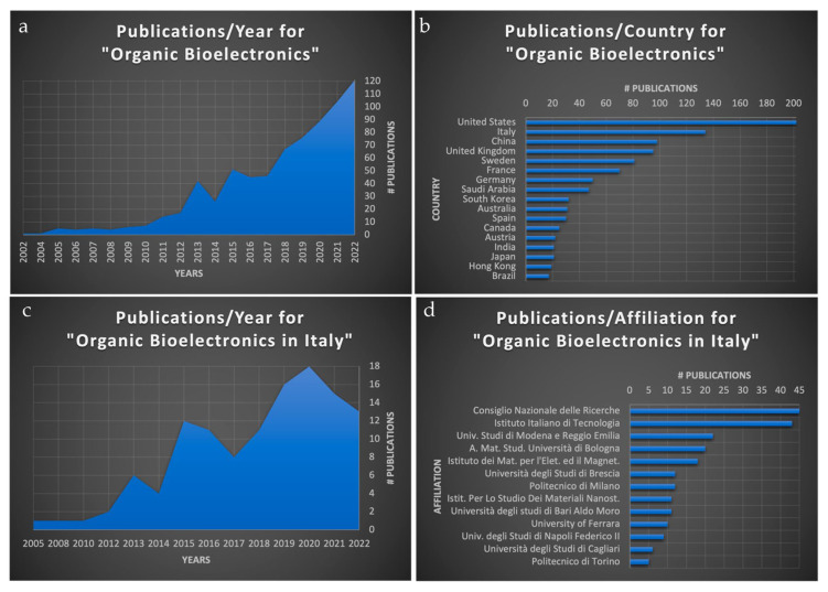
In recent years, studies concerning Organic Bioelectronics have had a constant growth due to the interest in disciplines such as medicine, biology and food safety in connecting the digital world with the biological one. Specific interests can be found in organic neuromorphic devices and organic transistor sensors, which are rapidly growing due to their low cost, high sensitivity and biocompatibility. This trend is evident in the literature produced in Italy, which is full of breakthrough papers concerning organic transistors-based sensors and organic neuromorphic devices. Therefore, this review focuses on analyzing the Italian production in this field, its trend and possible future evolutions.

Keywords: Organic Bioelectronics; biosensing; neuromorphic.


Conflict of interest statement

The authors declare no conflict of interest.

Figures

Figure 1
Figure 1
(a): The number of publications per year considering the keyword “Organic Bioelectronics” in the last two decades (source scopus.com, accessed on 11 January 2023); (b): the number of publications per country considering the keyword “Organic Bioelectronics” in the last two decades (source scopus.com); (c): the number of Italian publications per year considering the keyword “Organic Bioelectronics” in the last two decades (source scopus.com); (d): the number of Italian publications as a function of the authors’ affiliation considering the keyword “Organic Bioelectronics” in the last two decades (source scopus.com).
Figure 2
Figure 2
Different OFET architectures. (a): Bottom Contact–Top Gate; (b): Bottom Contact–Bottom Gate; (c): Top Contact–Bottom Gate; (d): Top Contact–Top Gate.
Figure 3
Figure 3
(a): Schematic architecture of an OECT. Application of a positive gate voltage induces cation penetration in the OSC with consequent electrochemical doping. (b): Schematic architecture of an EGOFET. Application of negative gate voltage induces the accumulation of anions (cations) in the EDL at the semiconductor/electrolyte interface, which in turn induces an accumulation of holes in the semiconductor.
Figure 4
Figure 4
Schematic example of a standard micro-fabrication process employed for EGOT fabrication. (ae): lift-off process for the definition of source and drain electrodes; (fi): lift-off process for the definition of contacts passivation. (j) Optical picture of the final device. Copyright (2022) Wiley. Used with permission from M. Segantini et al., “Investigation and Modeling of the Electrical Bias Stress in Electrolyte-Gated Organic Transistors,” Adv. Electron. Mater., vol. 8, no. 7, 2022, Wiley [59].
Figure 5
Figure 5
(ac): Schematic fabrication process of fully printed, maskless OECT. (d): Picture of the device during the printing process. (e): Final devices on flexible, transparent substrate. (f): Micrograph of a finite device. Copyright (2022) Wiley. Used with permission from R. Granelli et al., “High-Performance Bioelectronic Circuits Integrated on Biodegradable and Compostable Substrates with Fully Printed Mask-Less Organic Electrochemical Transistors,” Small, vol. 18, no. 26, 2022, Wiley [7].
Figure 6
Figure 6
Functionalization strategy. (A): Top: Functionalized gate presenting a platinum layer on top of the carbon-printed gate enzyme (the cartoon representation is not to scale). Bottom: the reactions involved in the enzymatic detection of UA. (B): Normalized current variation at fixed VGS = 0.5 V, as a function of [UA] for OECT gated by a bare platinum gate (C/Pt, black dots) and at a platinum, further-functionalized gate with gelatin A and B (C/Pt/GelB/GelA, blue dots). (C): Normalized current variation as a function of [H2O2] for OECT gated by C/Pt (black dots) and by C/Pt/GelB/GelA (red dots) electrodes. Reprinted with permissions from [70].
Figure 7
Figure 7
(a): Schematic of the hairpin-probe-sensing mechanism [106]. (b): (A) 3D schematic of the device. (B) Schematic of the gate functionalization with biotinylated single-strand oligonucleotides. Reprinted with permission from https://pubs.acs.org/doi/10.1021/acssensors.0c00694 [104]. Further permission related to the material excerpted should be directed to the ACS.
Figure 8
Figure 8
(a): OCMEFET placed on the skin of a finger, demonstrating its good conformability [113]. (b): OECT patterned on polyethylene naphthalate foil bent with a radius of 6 mm to mimic a real-life application; interfacing the sensor with a portable, handheld, battery-powered electronic readout from Elements srl company, wirelessly transmitting the current signal to a smartphone application [115].
Figure 9
Figure 9
(A): Schematic of the front view and top view of a Tweel OECT. (B): Representative images of the fluorescence assay and the increasing doxorubicin concentration. The number of dead cells increase, increasing the drug concentration. (C): Kinetics of the source/drain current as a function of doxorubicin concentration. (D,E): Comparison between calculated γ parameter and results from the fluorescence and MTT assay [121].
Figure 10
Figure 10
Scheme of the three-electrode electronic element based on polyaniline. Reprinted from Demin, V.A. et al. “Electrochemical model of the polyaniline based organic memristive device”. Journal of Applied Physics 116.6 (2014): 064507, with the permission of AIP Publishing [145].
Figure 11
Figure 11
(a): OMDs scheme and electrical configuration: gold source and drain electrodes are in contact with a polymeric thin film of polyaniline (PANI). The latter is in direct contact with an electrolytic solution in which a silver wire is inserted as a gate electrode. Source and drain electrodes are biased with a VSD voltage value, which induces resistivity variations in ISD and IGS currents; (b): ISD response to VSD variations as a function of the scan speed. In the inset, there are related IGS responses. Copyright 2021 Wiley. Used with permission from Battistoni S. et al. “The role of the internal capacitance in organic memristive device for neuromorphic and sensing applications.” Advanced Electronic Materials 7.11 (2021): 2100494 John Wiley and Sons [130].
Figure 12
Figure 12
(a): Kinetics of changes in conductivity and gate charge in time under the applied voltages of −0.2 and +0.7 V. The red vertical line indicates the voltage change. (b): Heatmap of absorbance evolution in time within the active zone under applied voltages of −0.2 and +0.7 V. The grey horizontal line is the silver wire. The “source” electrode is on the top, the “drain” on the bottom of the panel [141]. Reproduced from D.A. Lapkin, A.N. Korovin, S.N. Malakhov, A.V. Emelyanov, V.A. Demin, and V.V. Erokhin, “Optical monitoring of the resistive states of a polyaniline-based memristive device”, Adv. Electron. Mater, 6, 2000511 (2020), © 2020 Wiley-VCH GmbH.
Figure 13
Figure 13
Endurance of microscale OMDs for different switching cycles from high-conductive (“on”) to low-conductive (“off”) states. Reprinted from Lapkin, D. A. et al. “Polyaniline-based memristive microdevice with high switching rate and endurance.” Applied Physics Letters 112.4 (2018): 043302, with the permission of AIP Publishing [133].
Figure 14
Figure 14
Parylene repetitive unit.
Figure 15
Figure 15
Electrophysical and structural characterization of the M/PPX/ITO structures. (a): I–V cyclic characteristics showing the typical bipolar resistance-switching behavior of the Cu/PPX/ITO sample during 7 cycles (cycle-to-cycle variability); the average curve is highlighted in bold. (b): I–V characteristics collected in 8 different Cu/PPX/ITO devices (device-to-device variability, the fifth of ten cycles is shown for each); the average characteristics are highlighted in bold. (c): Cumulative probabilities of USET and URESET switching voltages and their coefficients of variation (CV) for ~100 I–V cyclic characteristics measured in the samples with copper (red) and silver (black) top electrodes. (d): Temperature dependence of the low-resistance state of the Cu/PPX/ITO structure. (e): Cross-sectional TEM image of the Cu/PPX/ITO sandwich structure. (f): Enlarged image of the area highlighted by the rectangle in (e), showing roughness of the Cu/PPX interface [154]. Reprinted from Organic Electronics, Vol. 74, A.A. Minnekhanov, B.S. Shvetsov, M.M. Martyshov, K.E. Nikiruy, E.V. Kukueva, M.Y. Presnyakov, P.A. Forsh, V.V. Rylkov, V.V. Erokhin, V.A. Demin, and A.V. Emelyanov, “On the resistive switching mechanism of parylene-based memristive devices”, pages 89–95, Copyright (2019), with permission from Elsevier.
Figure 16
Figure 16
Schematic representation of the evolution of metal bridges (conducting filaments) in Cu/PPX/ITO memristive devices and the consequent quantum conductance effect. (a): Fragment of the pristine sandwich structure, having some surface irregularities on the top electrode. The orange pellets represent Cu atoms. (b): A positive voltage is applied to the top electrode of the structure; copper ions begin to move to the cathode (ITO) under the action of an electric field. (c): Copper ions reach the bottom electrode and reduce, so a conductive filament begins to grow. (d): The conductive filament is completely formed; quantized conductance is not observed. (e): A negative voltage is applied to the top electrode; copper ions begin to move backward to it. A quasi-point contact is formed, so the conductance is quantized, becoming approximately equal to G0. (f): The conductive filament has ruptured; conductance is much less than G0 [154]. Reprinted from Organic Electronics, Vol. 74, A.A. Minnekhanov, B.S. Shvetsov, M.M. Martyshov, K.E. Nikiruy, E.V. Kukueva, M.Y. Presnyakov, P.A. Forsh, V.V. Rylkov,, V.V. Erokhin, V.A. Demin, and A.V. Emelyanov, “On the resistive switching mechanism of parylene-based memristive devices”, pages 89–95, Copyright (2019), with permission from Elsevier.
Figure 17
Figure 17
Emulation of synaptic long-term potentiation (LTP) and long-term depression (LTD) with OMD as a function of the number of delivered voltage spikes. Copyright 2021 Wiley. Used with permission from Battistoni, Silvia et al. “The role of the internal capacitance in organic memristive device for neuromorphic and sensing applications.” Advanced Electronic Materials 7.11 (2021): 2100494 John Wiley and Sons [130].
Figure 18
Figure 18
Response of OECT with a graphene-like gate electrode to a series of cumulative pulses (100 pulses at +1 V and >100 pulses at −0.5 V) as a function of the electrolyte composition. In the inset: plot of the time needed to reset the current to its initial value. Battistoni, Silvia et al. “Synaptic response in organic electrochemical transistor gated by a graphene electrode.” Flexible and Printed Electronics 4.4 (2019): 044002, DOI 10.1088/2058-8585 [2] © IOP Publishing. Reproduced with permission. All rights reserved.
Figure 19
Figure 19
(a): Schematic representation of an implantable PEDOT:PSS artificial synapse; (b): expression of the facilitative or depressive STP behavior upon frequency variation. Reprinted ad adapted from [160]: Calandra Sebastianella, Gioacchino et al. “Implantable Organic Artificial Synapses Exhibiting Crossover between Depressive and Facilitative Plasticity Response.” Advanced Electronic Materials 7.12 (2021): 2100755 under a Creative Commons license.
Figure 20
Figure 20
Spatio-temporal integration capabilities of OMDs: (a): Circuit-wiring diagram for operating the OMD for the temporal integration function. (b): Current output (black curve) and voltage profile (blue curve) used for the temporal integration. (c): Circuit-wiring diagram for operating the OMD for the spatial integration function. (d): Results of the spatial integration test. OMDs can integrate (bottom panel) two different “presynaptic” inputs (top and middle panels). Copyright 2021 Wiley. Used with permission from Battistoni, Silvia et al. “The role of the internal capacitance in organic memristive device for neuromorphic and sensing applications.” Advanced Electronic Materials 7.11 (2021): 2100494 John Wiley and Sons [130].
Figure 21
Figure 21
(a): Geometrical representation of the linear separability of objects, corresponding to NAND logic function [167]. Reprinted from Organic Electronics, Vol. 25, V.A. Demin, V. Erokhin, A.V. Emelyanov, S. Battistoni, G. Baldi, S. Iannotta, P.K. Kashkarov, and M.V. Kovalchuk, “Hardware elementary perceptron based on polyaniline memristive devices”, pages 16–20, Copyright (2015), with permission from Elsevier ; (b): Scheme of the elementary single-layer perceptron, based on organic memristive device [167]. Reprinted from Organic Electronics, Vol. 25, V.A. Demin, V. Erokhin, A.V. Emelyanov, S. Battistoni, G. Baldi, S. Iannotta, P.K. Kashkarov, and M.V. Kovalchuk, “Hardware elementary perceptron based on polyaniline memristive devices”, pages 16–20, Copyright (2015), with permission from Elsevier.
Figure 22
Figure 22
(a): Scheme of the double-layer perceptron; Experimental data. (b): Output signal within the epochs before (left) and after (right) training and expected output signal (dotted). (c): Synaptic weights and (d): corresponding feature plane partition (area above and below the plane y = 4,5 is the class “1” and “0”, correspondingly). Obtained separating planes are implemented by corresponding neurons in the first layer [169]. Reprinted from A.V. Emelyanov, D.A. Lapkin, V.A. Demin, V.V. Erokhin, S. Battistoni, G. Baldi, A. Dimonte, A.N. Korovin, S. Iannotta, P.K. Kashkarov, and M.V. Kovalchuk, “First step towards the realization of a double layer perceptron, based on organic memristive decices”, AIP Adv., 6, 111301 (2016) with the permission of AIP Publishing.
Figure 23
Figure 23
(a): Shapes of pre-synaptic (red line) and post-synaptic (black line) potential pulses. (b): Resulting voltage across the memristive element for the specific Δt = 200 s value [174]. Reprinted from Microelectronic Engineering, Vol. 185, D.A. Lapkin, A.V. Emelyanov, V.A. Demin, T.S. Berzina, and V.V. Erokhin, “Spike-timing-dependent plasticity of polyaniline-based memristive element”, pages 43–47, Copyright (2018), with permission from Elsevier; (c): STDP window for the memristive-device-related conductance changes for different ∆t delay values. The inset shows the shapes of pre-synaptic (black) and post-synaptic (red) potential pulses [143]. Reproduced with permission from N.V. Prudnikov, D.A. Lapkin, A.V. Emelyanov, A.A. Minnekhanov, Y.N. Malakhova, S.N. Chvalun, V.A. Demin, and V.V. Erokhin, “Associative STDP-like learning of neuromorphic circuits based on polyaniline memristive microdevices”, J. Phys. D: Appl. Phys., 53, 414001 (2020). Copyright (2020) IOP Publishing, Ltd.
Figure 24
Figure 24
STDP window of Cu/PPX/ITO memristive structures (for various initial conductance values) obtained with heteropolar (a): bi-rectangular and (b): bi-triangular spike pulses shown in the figure insets. Post-synaptic spikes were applied after (before) pre-synaptic ones with a varying delay time Δt. Every point of the curves is an average of 10 recorded experimental values [136]. Reproduced from A.A. Minnekhanov, A.V. Emelyanov, D.A. Lapkin, K.E. Nikiruy, B.S. Shvetsov, A.A. Nesmelov, V.V. Rylkov, V.A. Demin, and V.V. Erokhin, “Parylene based memristive devices with multilevel resistive switching for neuromorphic applications”, Sci. Rep., 9, 10800 (2019).
Figure 25
Figure 25
STDP-like learning memristive Pavlov’s dog implementation. (a): The electrical schematic diagram: N1—the first pre-neuron, spiking after the “food”-related stimulus; N2—the second pre-neuron, spiking after the “bell” stimulus; N3—the post-neuron, which spikes when the total input current exceeds the threshold; R—a resistor with a constant resistance value of R = 2 kΩ; M—a memristive element, initially in the Roff = 20 kΩ resistive state. A post-spike is generated unconditionally after a spike comes from N1 and under the condition that the memristor current exceeds Ith after a spike comes from N2. (b): An example of the spike pattern applied to the inputs of the scheme: 1—the initial pulse (first Epoch) on the resistor (R) (unconditioned stimulus), resulting in post-spike (P) 2, which in turn comes to the memristive device (M) as pulse 3 (dashed) in the inverted form; 4—the pulse on the memristive device, initially without post-neuron activity; 5—simultaneous pulses on the resistor and the memristive device, which result in post-spike 6 leading to the training pulse 7 (dashed); 8—a post-spike as a result of the conditioned stimulus when the training is completed (Epoch n, where n is equal to or above the number of epochs required for successful conditioning) [136]. Reproduced from A.A. Minnekhanov, A.V. Emelyanov, D.A. Lapkin, K.E. Nikiruy, B.S. Shvetsov, A.A. Nesmelov, V.V. Rylkov, V.A. Demin, and V.V. Erokhin, “Parylene based memristive devices with multilevel resistive switching for neuromorphic applications”, Sci. Rep., 9, 10800 (2019).
Figure 26
Figure 26
Activity-dependent coupling of neurons by the organic memristive device. (a): Infrared differential interference contrast microphotograph of a P7 rat brain slice with visually identified L5/6 neocortical cells (Cell1,2) recorded simultaneously. (b): Simplified electrical scheme of two patch-clamp amplifier headstages (Patch1,2): 1,3—patch-clamp holding inputs; 2,4—patch-clamp primary outputs; and an organic memristive device-based circuit (5 × 5 mm) connecting two neurons. (c,d): Traces of current-clamp recordings from Cells 1 and 2 before (c): and after (d): coupling through the organic memristive device. Traces 1–4 correspond to the inputs/outputs as labeled in (b). Note that prior to coupling through the organic memristive device (c), APs in either neuron failed to evoke responses in the other neuron, indicating that these cells were not connected by natural synapses. After the connection of Cells 1 and 2 through an organic memristive device (d), the efficacy of coupling progressively increases with each consecutive depolarizing step/AP in Cell 1. 500 traces (color coded by sweep #) are aligned with suprathreshold depolarizing steps delivered to Cell 1. Bottom plot, organic memristive device resistance as a function of the sweep #. Dashed lines indicate the first sweep when Cell 2 started firing. (e): Corresponding plots of the activity-dependent change in spike probability in Cell 2 (top), spike delay of Cell 2 from Cell 1 (middle) and spike delay jitter in Cell 2 (bottom). (f): Histogram of the spike delay in Cell 2 from Cell 1 calculated for three OMD-coupled cell pairs (777 spikes) [179]. Reprinted from E. Juzekaeva, A. Nasretdinov, S. Battistoni, T. Berzina, S. Iannotta, R. Khazipov, V. Erokhin, and M. Mukhtarov, “Coupling cortical neurons through electronic memristive synapse”, Adv. Mater. Technol., 4, 1800350 (2019), John Wiley and Sons, © 2018 WILEY-VCH Verlag GmbH & Co. KGaA, Weinheim.
Figure 27
Figure 27
Synchronous oscillations in the natural neuron network where two cortex neurons were coupled through the organic memristive device. (a): Current-clamp recordings from Cell 1 (blue) and Cell 2 (red). Parts of traces outlined by dashed boxes before and after spike coupling through organic memristive device are shown on expanded time scales on the right. The horizontal dashed line indicates Cell 2 spike threshold. (b): Corresponding membrane potential spectrograms in Cells 1 and 2. (c): Power spectrum density plots of the membrane potential in Cells 1 and 2 before (top) and after (bottom) spike-coupling through the organic memristive device (confidence interval is shadowed; n = 3 pairs). (d): Frequency of spikes (top) in Cell 1 (blue) and Cell 2 (red) calculated for the 10 s bin intervals from the recordings shown in a and the corresponding values of the organic memristive device resistance (bottom). Dashed lines indicate the onset of spike-coupling between Cells 1 and 2. (e): Example of 65 normalized spikes (top) recorded in Cell 1 (blue traces) and Cell 2 (red traces) and the histogram of the spike delay in Cell 2 from Cell 1 (bottom), data from three organic memristive device-coupled cell pairs (633 spikes) are pooled together [179]. Reprinted from E. Juzekaeva, A. Nasretdinov, S. Battistoni, T. Berzina, S. Iannotta, R. Khazipov, V. Erokhin, and M. Mukhtarov, “Coupling cortical neurons through electronic memristive synapse”, Adv. Mater. Technol., 4, 1800350 (2019), John Wiley and Sons, © 2018 WILEY-VCH Verlag GmbH & Co. KGaA, Weinheim.

References

    1. D’Angelo P., Tarabella G., Romeo A., Marasso S.L., Cocuzza M., Peruzzi C., Vurro D., Carotenuto G., Iannotta S. Nanomolar Detection of the Antitumor Drug Tamoxifen by Flexible Organic Electrochemical Devices. AIP Conf. Proc. 2018;1990:020015. doi: 10.1063/1.5047769. - DOI
    1. Battistoni S., Peruzzi C., Verna A., Marasso S.L., Cocuzza M., Erokhin V., Iannotta S. Synaptic Response in Organic Electrochemical Transistor Gated by a Graphene Electrode. Flex. Print. Electron. 2019;4:044002. doi: 10.1088/2058-8585/ab4dce. - DOI
    1. Sajapin R., Vurro D., D’Angelo P., Tarabella G., Marasso S.L., Cocuzza M., Botti M., Buttrini M., Calderaro A., Berzina T., et al. Aerosol Jet Printed Organic Memristive Microdevices Based on a Chitosan: PANI Composite Conductive Channel. ACS Appl. Electron. Mater. 2022;4:5875–5883. doi: 10.1021/acsaelm.2c01047. - DOI
    1. Cavallo A., Losi P., Buscemi M., Al Kayal T., Beccatelli M., Soldani G., Coppedè N. Biocompatible Organic Electrochemical Transistor on Polymeric Scaffold for Wound Healing Monitoring. Flex. Print. Electron. 2022;7:035009. doi: 10.1088/2058-8585/ac84ec. - DOI
    1. Gentile F., Vurro F., Janni M., Manfredi R., Cellini F., Petrozza A., Zappettini A., Coppedè N. A Biomimetic, Biocompatible OECT Sensor for the Real-Time Measurement of Concentration and Saturation of Ions in Plant Sap. Adv. Electron. Mater. 2022;8:200092. doi: 10.1002/aelm.202200092. - DOI

LinkOut - more resources