. 2023 Feb 27;14(1):1103.
doi: 10.1038/s41467-023-36722-7.

Laser printed microelectronics

Affiliations

Laser printed microelectronics

Liang Yang et al. Nat Commun. .

Abstract

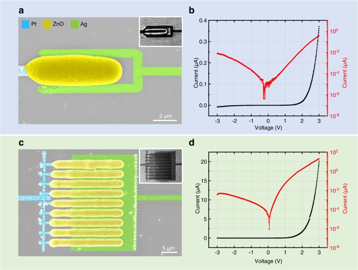
Printed organic and inorganic electronics continue to be of large interest for sensors, bioelectronics, and security applications. Many printing techniques have been investigated, albeit often with typical minimum feature sizes in the tens of micrometer range and requiring post-processing procedures at elevated temperatures to enhance the performance of functional materials. Herein, we introduce laser printing with three different inks, for the semiconductor ZnO and the metals Pt and Ag, as a facile process for fabricating printed functional electronic devices with minimum feature sizes below 1 µm. The ZnO printing is based on laser-induced hydrothermal synthesis. Importantly, no sintering of any sort needs to be performed after laser printing for any of the three materials. To demonstrate the versatility of our approach, we show functional diodes, memristors, and a physically unclonable function based on a 6 × 6 memristor crossbar architecture. In addition, we realize functional transistors by combining laser printing and inkjet printing.


Conflict of interest statement

The authors declare no competing interests.

Figures

Fig. 1
Fig. 1. Direct laser printing of microelectronic structures.
a Scheme of a femtosecond laser centered around 780 nm wavelength that is focused into the Pt ink for multi-photon reduction of Pt. b A continuous-wave laser at 532 nm wavelength is focused onto a Pt wire immersed in the ZnO ink for the local photothermal synthesis of ZnO. c The 780 nm femtosecond laser is focused above the ZnO layer within the Ag ink for further multi-photon reduction of Ag. df Scanning-electron micrographs of laser-printed structures corresponding to the process steps ac, colored according to the different materials involved. The inset in e reveals the surface of a laser-printed ZnO structure.
Fig. 2
Fig. 2. Controlling the geometry of laser-printed ZnO.
a Scanning-electron micrograph of ZnO deposited on Pt wires by point exposure of a 532 nm wavelength continuous-wave laser. The laser power is fixed at P=30%P0, with P0=21.5mW, while the exposure time increases from Δt=2ms to 4096ms from left to right. b, c Quantitative investigation of the geometrical size of laser-printed ZnO by controlling P and Δt, for pH values of 9.86 ± 0.01 and 10.00 ± 0.02, respectively. d Linewidth of laser-printed ZnO wires versus P for three different pH values of the ZnO ink, as indicated in the legend. The data points in bd are mean values from 20 measures.
Fig. 3
Fig. 3. Laser-printed Pt–ZnO–Ag diodes.
a Scanning-electron micrograph of a single diode composed of Pt and Ag wires (see coloration) and a ZnO bar in between. Inset: optical transmission micrograph of the same structure. b Corresponding measured current-voltage characteristics on a linear (left, black) and a logarithmic scale (right, red). c Scanning-electron micrograph of a diode with interdigitated metal contacts. Inset: optical transmission micrograph. d Current–voltage measurement for the diode in c.
Fig. 4
Fig. 4. Laser-printed crossbar Pt–ZnO–Ag memristor device.
a 1×6 crossbar structure with varying ZnO linewidths, realized by controlling the laser power during laser printing. The electrical performance of the crossbar structure is determined by the dimensions of the ZnO layer. b Scheme of the mechanism at work. c Current–voltage characteristics of a single memristor for 300 cycles. The forming process (black), cycle number 100 (red), cycle number 200 (blue), and cycle number 300 (green) are emphasized by color, all other cycles are shown in gray. d Histograms of the set and reset voltages measured in the 300 cycles in panel c. e The stable retention performance of both resistive states on a timescale of up to 104s. f, Resistive switching endurance of a single memristor under short-pulse-voltage mode (see inset) over 700 cycles.
Fig. 5
Fig. 5. Laser-printed Pt-ZnO-Ag security circuits.
a Schematic of an embedded hardware-based security primitive, based on a physically unclonable function (PUF). b Optical micrograph of a laser-printed 6×6 crossbar array with contact pads. c Scanning-electron micrograph of a laser-printed 6×6 crossbar array, showing a period of 1.5 µm in both, horizontal and vertical directions. The memristive devices are located at the wire crossing junctions. d Activation of the 36 memristor cells by sweeping a voltage from 0V10V4V0V. The inset shows the set process of the 36 memristor cells for positive voltages, with the compliance current set to 1mA. e False-color representation of the read-out currents Iread from the 6×6 array. f Retention performance of Iread over a timespan of 60 s. g Circuit architecture around the core of the memristor-PUF. h Bit-array distribution corresponding to the 6×6 crossbar array. i Schematic of the evaluated bit errors over 300 cycles.

References

    1. Park S, et al. Self-powered ultra-flexible electronics via nano-grating-patterned organic photovoltaics. Nature. 2018;561:516–521. doi: 10.1038/s41586-018-0536-x. - DOI - PubMed
    1. Fabiano S, Facchetti A. Stretchable helix-structured fibre electronics. Nat. Electron. 2021;4:864–865. doi: 10.1038/s41928-021-00693-8. - DOI
    1. Zschieschang U, Waizmann U, Weis J, Borchert JW, Klauk H. Nanoscale flexible organic thin-film transistors. Sci. Adv. 2022;8:eabm9845. doi: 10.1126/sciadv.abm9845. - DOI - PMC - PubMed
    1. Shulga AG, et al. Electroluminescence generation in PbS quantum dot light-emitting field-effect transistors with solid-state gating. ACS Nano. 2018;12:12805–12813. doi: 10.1021/acsnano.8b07938. - DOI - PMC - PubMed
    1. Liu F, et al. Printed synaptic transistors based electronic skin for robots to feel and learn. Sci. Robot. 2022;7:eabl7286. doi: 10.1126/scirobotics.abl7286. - DOI - PubMed

LinkOut - more resources