

A 21.4 pW Subthreshold Voltage Reference with 0.020 %/V Line Sensitivity Using DIBL Compensation
- PMID: 36850459
- PMCID: PMC9963272
- DOI: 10.3390/s23041862
A 21.4 pW Subthreshold Voltage Reference with 0.020 %/V Line Sensitivity Using DIBL Compensation
Abstract
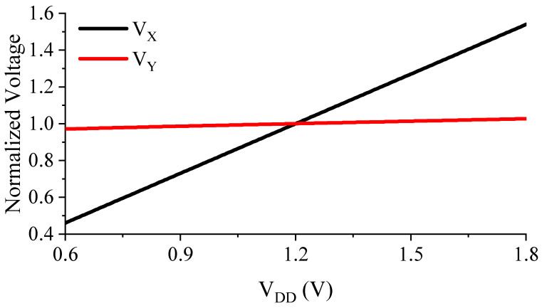
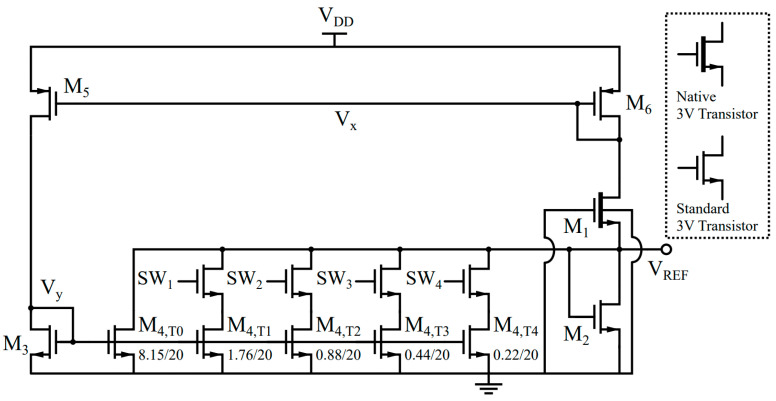
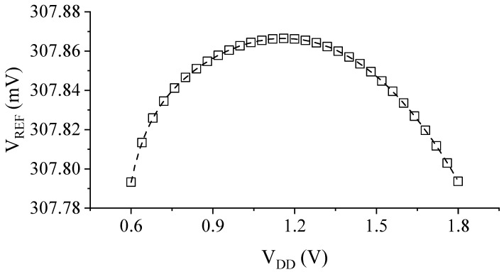
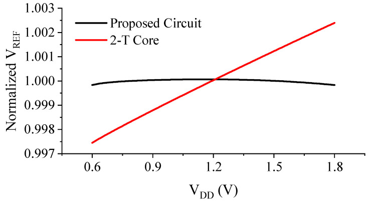
This paper presents an ultra-low-power voltage reference designed in 180 nm CMOS technology. To achieve near-zero line sensitivity, a two-transistor (2-T) voltage reference is biased with a current source to cancel the drain-induced barrier-lowering (DIBL) effect of the 2-T core, thus improving the line sensitivity. This compensation circuit achieves a Monte-Carlo-simulated line sensitivity of 0.035 %/V in a supply range of 0.6 to 1.8 V, while generating a reference voltage of 307.8 mV, with 21.4 pW power consumption. The simulated power supply rejection ratio (PSRR) is -54 dB at 100 Hz. It also achieves a temperature coefficient of 24.8 ppm/°C in a temperature range of -20 to 80 °C, with a projected area of 0.003 mm2.
Keywords: DIBL effect; line sensitivity; subthreshold voltage reference; temperature coefficient; ultra-low-power.
Conflict of interest statement
The authors declare no conflict of interest.
Figures


References
-
- Chen K., Petruzzi L., Hulfachor R., Onabajo M. A 1.16-V 5.8-to-13.5-ppm/°C Curvature-Compensated CMOS Bandgap Reference Circuit With a Shared Offset-Cancellation Method for Internal Amplifiers. IEEE J. Solid-State Circuits. 2021;56:267–276. doi: 10.1109/JSSC.2020.3033467. - DOI
-
- Boo J.-H., Cho K.-I., Kim H.-J., Lim J.-G., Kwak Y.-S., Lee S.-H., Ahn G.-C. A Single-Trim Switched Capacitor CMOS Bandgap Reference With a 3σ Inaccuracy of +0.02%, −0.12% for Battery-Monitoring Applications. IEEE J. Solid-State Circuits. 2021;56:1197–1206. doi: 10.1109/JSSC.2020.3044165. - DOI
-
- Kim M., Cho S. A Single BJT Bandgap Reference with Frequency Compensation Exploiting Mirror Pole. IEEE J. Solid-State Circuits. 2021;56:2902–2912. doi: 10.1109/JSSC.2021.3093583. - DOI
-
- Seok M., Kim G., Blaauw D., Sylvester D. A PorTable 2-Transistor Picowatt Temperature-Compensated Voltage Reference Operating at 0.5 V. IEEE J. Solid-State Circuits. 2012;47:2534–2545. doi: 10.1109/JSSC.2012.2206683. - DOI
-
- Lin J., Wang L., Zhan C., Lu Y. A 1-nW Ultra-Low Voltage Subthreshold CMOS Voltage Reference With 0.0154%/V Line Sensitivity. IEEE Trans. Circuits Syst. II Express Briefs. 2019;66:1653–1657. doi: 10.1109/TCSII.2019.2920693. - DOI
LinkOut - more resources
Full Text Sources
Miscellaneous
