

Sensitivity of Al-Doped Zinc-Oxide Extended Gate Field Effect Transistors to Low-Dose X-ray Radiation
- PMID: 36902983
- PMCID: PMC10004138
- DOI: 10.3390/ma16051868
Sensitivity of Al-Doped Zinc-Oxide Extended Gate Field Effect Transistors to Low-Dose X-ray Radiation
Abstract
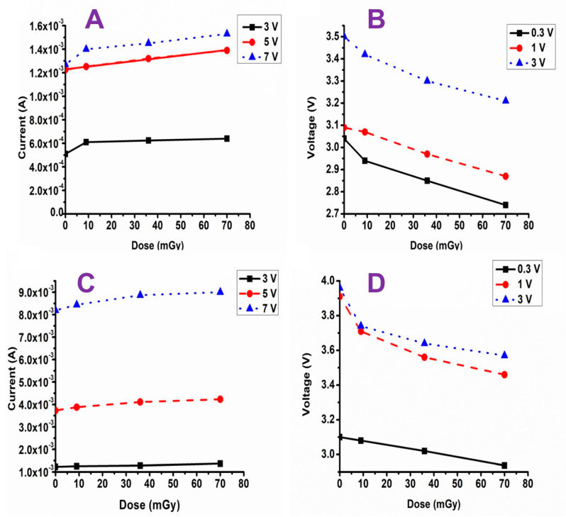
Herein, we investigated the applicability of thick film and bulk disk forms of aluminum-doped zinc oxide (AZO) for low-dose X-ray radiation dosimetry using the extended gate field effect transistor (EGFET) configuration. The samples were fabricated using the chemical bath deposition (CBD) technique. A thick film of AZO was deposited on a glass substrate, while the bulk disk form was prepared by pressing the collected powders. The prepared samples were characterized via X-ray diffraction (XRD) and field emission scanning electron microscope (FESEM) to determine the crystallinity and surface morphology. The analyses show that the samples are crystalline and comprise nanosheets of varying sizes. The EGFET devices were exposed to different X-ray radiation doses, then characterized by measuring the I-V characteristics pre- and post-irradiation. The measurements revealed an increase in the values of drain-source currents with radiation doses. To study the detection efficiency of the device, various bias voltages were also tested for the linear and saturation regimes. Performance parameters of the devices, such as sensitivity to X-radiation exposure and different gate bias voltage, were found to depend highly on the device geometry. The bulk disk type appears to be more radiation-sensitive than the AZO thick film. Furthermore, boosting the bias voltage increased the sensitivity of both devices.
Keywords: AZO; EGFET; MOSFET; chemical bath deposition; radiation detector.
Conflict of interest statement
The authors declare no conflict of interest.
Figures


References
-
- Gordillo G., Calderon C. Properties of ZnO thin films prepared by reactive evaporation. Sol. Energy Mater. Sol. Cells. 2001;69:251–260. doi: 10.1016/S0927-0248(00)00394-9. - DOI
-
- Hiramatsu M., Imaeda K., Horio N., Nawata M. Transparent conducting ZnO thin films prepared by XeCl excimer laser ablation. J. Vac. Sci. Technol. A Vac. Surf. Film. 1998;16:669–673. doi: 10.1116/1.581085. - DOI
-
- Zhang W., He D., Liu Z., Sun L., Fu Z. Preparation of transparent conducting Al-doped ZnO thin films by single source chemical vapor deposition. J. Optoelectron. Adv. Mater–Rapid Commun. 2010;4:1651–1654.
Grants and funding
LinkOut - more resources
Full Text Sources
