. 2023 Feb 23;8(9):8263-8275.
doi: 10.1021/acsomega.2c06475. eCollection 2023 Mar 7.

About the Shape of the Crystallization Front of the Semiconductor Nanowires

Affiliations

About the Shape of the Crystallization Front of the Semiconductor Nanowires

Valery A Nebol'sin et al. ACS Omega. .

Abstract

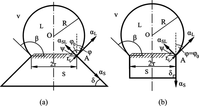
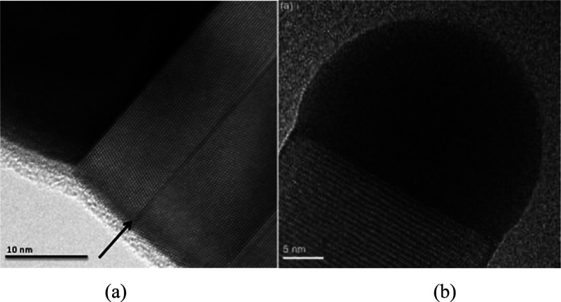
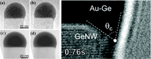
During the nanowire (NW) formation, the growth steps reaching the crystallization front (CF) under the catalytic drop are either absorbed by the three-phase line or accumulated in front of it, curving the surface of the front. In this paper, we have analyzed the conditions leading to a change of shape of the crystallization front of the NWs under the catalyst drop as well as the reasons for the formation of atomically smooth (singular) and curved (nonsingular) regions. A model explaining the curvature of the crystallization front under the drop in the process of NW growth is proposed. The model demonstrates that under conditions of good wettability of the crystalline surface with a catalytic liquid and nucleation at regular places of the growing NW face, a metastable equilibrium at the CF near the three-phase line is achieved due to the thermodynamic size effect of reduction of overcooling (supersaturation). This metastable equilibrium results in the curvature of the CF. The CF curvature depends on the NW radius and the level of overcooling (supersaturation) in the droplet. During this process, the low-index inclined facets adjacent to the wetting perimeter of the catalyst drop may appear on the curved CF.


Conflict of interest statement

The authors declare no competing financial interest.

Figures

Figure 1
Figure 1
Time dependencies of the contact angle θ during wetting of {111} Si substrates by Sn (line 1), Cu (line 2), Ag (line 3), and Au (line 4) drops (a) and alloys Sn + 5.0 atom % Si (line 1), Zn + 15.0 atom % Si (line 2), Cu + 36.1 atom % Si (line 3), and Au + 38.4 atom % Si (line 4) (b) at 1473 K in the stream of H2.
Figure 2
Figure 2
Etched cross-section of Si⟨111⟩ NW doped with boron in the process of growth through droplets Cu–Si at T = 1273 K. The image clearly shows a flat crystallization front, represented by a transverse close-packed face of the {111} family.
Figure 3
Figure 3
Thin sections of the Si NWs illustrate that at the initial growth stage, the CF is concave (a) and then becomes flat (b, c). The capture of a two-component alloy by a moving front during rapid NW crystallization is shown in (b) and (c) photos.
Figure 4
Figure 4
SEM image of the curved section of a nanowire crystallization front near the three-phase line in the Ag–Si system.
Figure 5
Figure 5
Morphology of the lateral surface of silicon NW, consisting of sickle-shaped alternating regions. Each section is a step cut by a plane of {111} and has a curved isotropic end.
Figure 6
Figure 6
Angular (orientational) dependence of the SFSE αS, illustrating the anisotropy of the crystal SFSE in the vicinity of the singular face with small crystallographic indices {hkl}., Reprinted with permission from Burton, W. K.; Cabrera, N.; Frank, F. C. The Growth of Crystals and the Equilibrium of Their Surfaces. Philos. Trans. R. Soc., A 1951, 243, 299–358. Copyright 1951 The Royal Society (U.K.).
Figure 7
Figure 7
Change in free energy during crystallization from a small drop of a Me catalyst with a different R.
Figure 8
Figure 8
Relationship between the radius of the critical nucleus rN*, formed at regular surface sites under the catalyst drop, and overcooling of ΔT/TE.
Figure 9
Figure 9
Diagram of the three-phase interfaces, solid, liquid, and vaporous: (a) for the catalyst droplet at the top of the conical NW (0 < δ < 90°) and (b) for cylindrical NW (δ = 90°).
Figure 10
Figure 10
GaAs NWs with a zinc blende structure in the top part of the crystal predominantly have a transverse close-packed (1̅1̅1̅) B face (a), while those with a wurtzite structure have a (000̅1) face (b). Reprinted with permission from Harmand, J.-C.; Patriarche, G.; Glas, F.; Panciera, F.; Florea, I.; Maurice, J.-L.; Travers, L.; Ollivier, Y. Atomic Step Flow on a Nanofacet. Phys. Rev. Lett. 2018, 121 (16), 166101. Copyright 2018 American Physical Society. Reprinted from Dhalluin, F. Nanofils de Silicium: Dépôt chimique en phase vapeur assisté par catalyseurs métalliques et prémices d’intégration. Ph.D. Thesis, University of Grenoble: Francais, 2009; p 221. This figure was dedicated to the Public domain (HAL Open Science) by the creator. https://theses.hal.science/tel-00495316.
Figure 11
Figure 11
Left: frame-by-frame TEM images of the Si NW tops with a diameter of 23 nm, growing at T = 833 K and Si2H6 pressure p = 1.07 × 10⁻³ Pa with AuAl–Si particles (a, b) and Si NWs with a diameter of 60 nm, grown at T = 773 K and ∼Si2H6p = 1.33 × 10⁻³ Pa with AuGa–Si particles (c, d) illustrating the curvature of the crystallization front in the vicinity of the TL. Reprinted with permission from Wen, C.-Y.; Tersoff, J.; Hillerich, K.; Reuter, M.C.; Park, J. H. Periodically Changing Morphology of the Growth Interface in Si, Ge, and GaP Nanowires. Phys. Rev. Lett. 2011, 107, 025503. Copyright 2011 American Physical Society. Right: TEM image of Ge NW top showing the formation of a flat inclined face near the TL on a curved CF region in the Au–Ge system. Reprinted with permission from Gamalski, A. D.; Ducati, C.; Hofman, S. Cyclic Supersaturation and TPB Dynamics in Ge NW Growth. J. Phys. Chem. C 2011, 115, 4413–4417. Copyright 2011 American Chemical Society.
Figure 12
Figure 12
Frame-by-frame images of the change in the truncation area at the edge of the sapphire (α-Al2O3) NW, i.e., changes of the area of the singular inclined face adjacent to the TL. (a–f) Images were captured from a real-time movie at the elapsed times shown. (g) The difference image obtained by subtracting the video image (c) from (e). (h, i) Schematic illustration of the triple-junction configuration during local crystal growth on the (01̅14) facet (h) and at the end of growth (i). Reprinted with permission from Oh, S. H.; Chisholm, M.F.; Kauffman, Y.; Kaplan, W. D.; Luo, W.; Ruhcle, M.; Scheu, C. Oscillatory Mass Transport in Vapor–Liquid–Solid Growth of Sapphire Nanowires. Science 2010, 330 (6003), 489–493. Copyright 2010 The American Association for the Advancement of Science.
Figure 13
Figure 13
Scheme of different types of conjugation of the interfaces of three phases at the top of the NWs: (a) internal inclined close-packed facet AC adjacent to the TL appears on the CF; (b) the facet AC exits to the lateral surface of the NW; and (c) the formation of a sawtooth lateral surface ACD of the crystal.
Figure 14
Figure 14
Formation of critical nuclei in the form of a spherical segment of the same radius of curvature r* of the segmental surface and with the same contact angles γ on (a) the convex surface (ψ > 0), (b) the flat surface (ψ = 0), and (c) concave surface (ψ < 0) of the CF.
Figure 15
Figure 15
SEM image of Si NW, showing faceting of sidewall surface immediately below the catalyst droplet. Reprinted with from Dhalluin, F. Nanofils de Silicium: Dépôt chimique en phase vapeur assisté par catalyseurs métalliques et prémices d’intégration. Ph.D. Thesis, University of Grenoble: Francais, 2009; p 221. This figure was dedicated to the Public domain (HAL Open Science) by the creator. https://theses.hal.science/tel-00495316.

References

    1. Thelander C.; Agarwal P.; Brongersma S.; Eymery J.; Feiner L.; Forchel A.; Scheffler M.; Riess W.; Ohlsson B.; Gösele U.; Samuelson L. Nanowire Base One-Dimensional Electronics. Mater. Today 2006, 9, 28–35. 10.1016/S1369-7021(06)71651-0. - DOI
    1. Ishikawa F.; Buyanova I. A.. Novel Compound Semiconductor Nanowires: Materials, Devices and Applications; Pan Stanford Publishing: Singapore, 2018.
    1. Lieber C. M. Semiconductor Nanowires: A Platform For Nanoscience And Nanotechnology. MRS Bull. 2011, 36, 1063.10.1557/mrs.2011.269. - DOI - PMC - PubMed
    1. Natarajan C. M.; Tanner M. G.; Hadfield R. H. Superconductor Science And Technology Superconducting Nanowire Single-photon Detectors: Physics And Applications Superconducting Nanowire Single-photon Detectors: Physics and Applications. Supercond. Sci. Technol. 2012, 25, 06300110.1088/0953-2048/25/6/063001. - DOI
    1. Fang X.; Bando Y.; Gautam U. K.; Ye C.; Golberg D. Inorganic Semiconductor Nanostructures And Their Field-emission Applications. J. Mater. Chem. 2008, 18, 509–522. 10.1039/B712874F. - DOI