

New insights into APCVD grown monolayer MoS2 using time-domain terahertz spectroscopy
- PMID: 36914682
- PMCID: PMC10011412
- DOI: 10.1038/s41598-023-31102-z
New insights into APCVD grown monolayer MoS2 using time-domain terahertz spectroscopy
Abstract
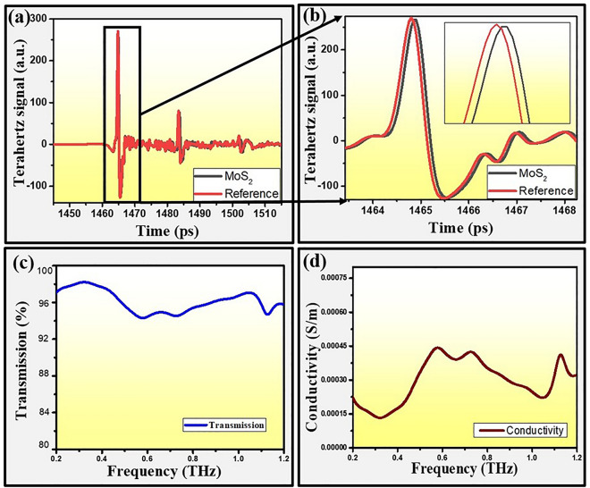
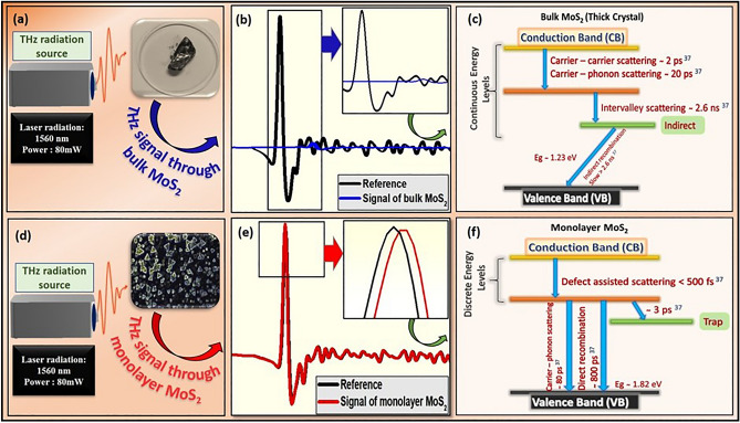
In modern era, wireless communications at ultrafast speed are need of the hour and search for its solution through cutting edge sciences is a new perspective. To address this issue, the data rates in order of terabits per second (TBPS) could be a key step for the realization of emerging sixth generation (6G) networks utilizing terahertz (THz) frequency regime. In this context, new class of transition metal dichalcogenides (TMDs) have been introduced as potential candidates for future generation wireless THz technology. Herein, a strategy has been adopted to synthesize high-quality monolayer of molybdenum di-sulfide (MoS2) using indigenously developed atmospheric pressure chemical vapor deposition (APCVD) set-up. Further, the time-domain transmission and sheet conductivity were studied as well as a plausible mechanism of terahertz response for monolayer MoS2 has been proposed and compared with bulk MoS2. Hence, the obtained results set a stepping stone to employ the monolayer MoS2 as potential quantum materials benefitting the next generation terahertz communication devices.
© 2023. The Author(s).
Conflict of interest statement
The authors declare no competing interests.
Figures

References
-
- Pawar AY, et al. Terahertz technology and its applications. Drug Invent. Today. 2013;5:157–163. doi: 10.1016/j.dit.2013.03.009. - DOI
-
- Serghiou D, et al. Terahertz channel propagation phenomena, measurement techniques and modeling for 6G wireless communication applications: A survey, open challenges and future research directions. IEEE Commun. Surv. Tutor. 2022;24:1957–1996. doi: 10.1109/COMST.2022.3205505. - DOI
-
- Chowdhury MZ, et al. 6G wireless communication systems: applications, requirements, technologies, challenges, and research directions. IEEE Open J. Commun. Soc. 2020;1:957–975. doi: 10.1109/OJCOMS.2020.3010270. - DOI
-
- Devi KM, Jana S, Chowdhury DR. Topological edge states in an all-dielectric terahertz photonic crystal. Opt. Mater. Express. 2021;11(8):2445–2458. doi: 10.1364/OME.427069. - DOI
LinkOut - more resources
Full Text Sources
