. 2023 Mar 28;17(6):6062-6072.
doi: 10.1021/acsnano.3c00670. Epub 2023 Mar 14.

Subnanometer-Wide Indium Selenide Nanoribbons

Affiliations

Subnanometer-Wide Indium Selenide Nanoribbons

William J Cull et al. ACS Nano. .

Abstract

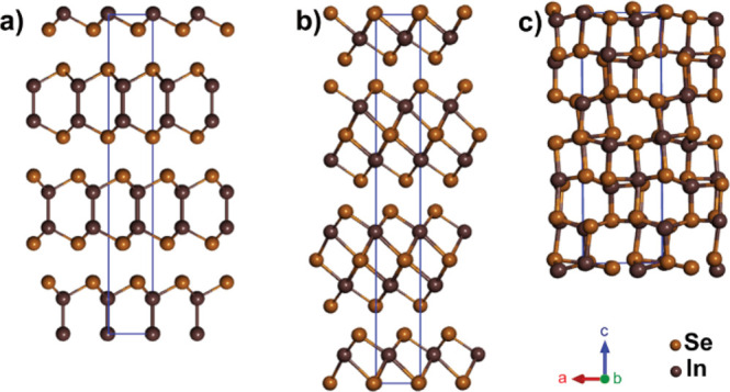
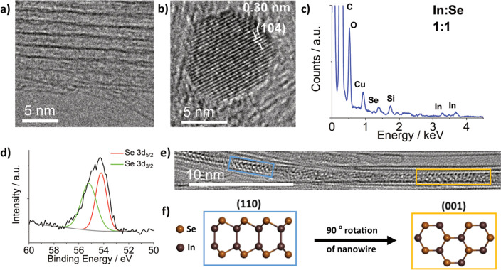
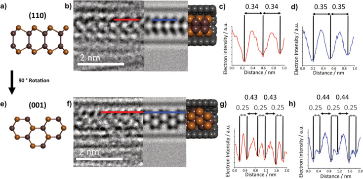
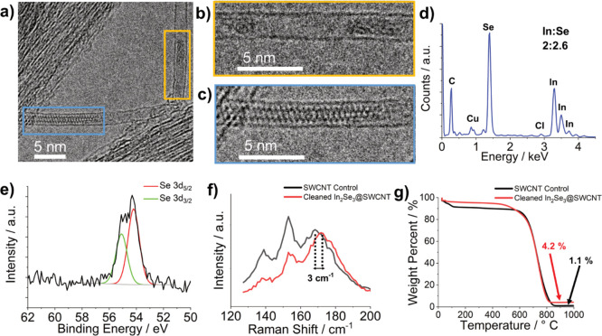
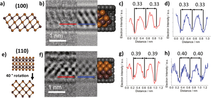
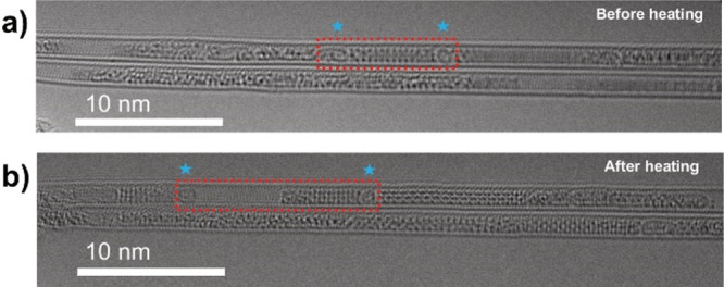
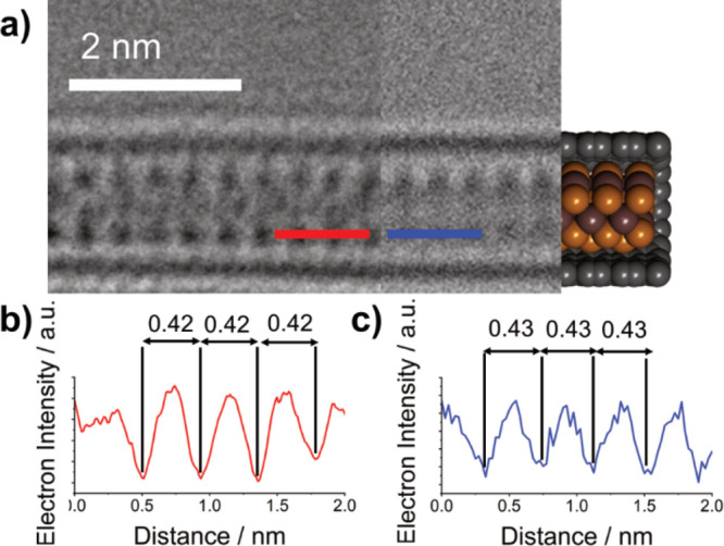
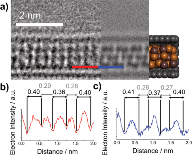
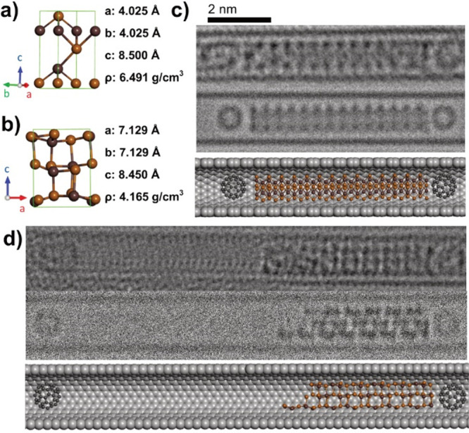
Indium selenides (InxSey) have been shown to retain several desirable properties, such as ferroelectricity, tunable photoluminescence through temperature-controlled phase changes, and high electron mobility when confined to two dimensions (2D). In this work we synthesize single-layer, ultrathin, subnanometer-wide InxSey by templated growth inside single-walled carbon nanotubes (SWCNTs). Despite the complex polymorphism of InxSey we show that the phase of the encapsulated material can be identified through comparison of experimental aberration-corrected transmission electron microscopy (AC-TEM) images and AC-TEM simulations of known structures of InxSey. We show that, by altering synthesis conditions, one of two different stoichiometries of sub-nm InxSey, namely InSe or β-In2Se3, can be prepared. Additionally, in situ AC-TEM heating experiments reveal that encapsulated β-In2Se3 undergoes a phase change to γ-In2Se3 above 400 °C. Further analysis of the encapsulated species is performed using X-ray photoelectron spectroscopy (XPS), thermogravimetric analysis (TGA), energy dispersive X-ray analysis (EDX), and Raman spectroscopy, corroborating the identities of the encapsulated species. These materials could provide a platform for ultrathin, subnanometer-wide phase-change nanoribbons with applications as nanoelectronic components.

Keywords: III−VI semiconductor; carbon nanotubes; indium selenide; nanoribbons; nanowires; phase change material.


Conflict of interest statement

The authors declare no competing financial interest.

Figures

Figure 1
Figure 1
Structures showing the (120) plane of bulk (a) γ-InSe, (b) β-In2Se3, and (c) γ-In2Se3 with their unit cells shown in blue.
Figure 2
Figure 2
Experimental results from the melt growth of γ-InSe inside SWCNTs: (a) 200 kV TEM of InSe@SWCNT; (b) 200 kV TEM of externally bound γ-InSe nanoparticle; (c) EDX spectrum of the area shown in (a); (d) XPS spectrum of InSe@SWCNT showing the Se 3d environment (e) 80 kV AC-TEM image of a single InSe nanoribbon inside a SWCNT with two distinct orientations highlighted in blue and yellow boxes; (f) molecular models created from single-layer InSe showing the proposed appearance of the two distinct orientations seen in (e), the (110) plane shown in the blue box and the (001) plane shown in the yellow box.
Figure 3
Figure 3
(a) Structural model of monolayer InSe in the (110) orientation. (b) Three-part composite image of an InSe nanoribbon inside a SWCNT, consisting of an AC-TEM image (left), a simulated TEM image (center), and molecular model (right). (c, d) Electron density profile maps in red, generated from the red line superimposed over the experimental AC-TEM image in (b), and in blue, generated from the blue line superimposed over the simulated TEM image in (b), with calculated interatomic distances highlighted in nm. (e–h) The same as (a–d), respectively, but for the (001) orientation of the same nanoribbon.
Scheme 1
Scheme 1. Reaction to Form Indium Sesquiselenide
Figure 4
Figure 4
(a) 200 kV TEM image of In2Se3@SWCNTs. (b, c) Digitally magnified TEM images of the yellow and blue areas, respectively, highlighted in (a). (d) EDX spectrum of a bundle of In2Se3@SWCNTs. (e) XPS spectrum of In2Se3@SWCNTs showing the Se 3d environment. (f) Raman analysis of In2Se3@SWCNTs (red) and control SWCNTs (black), showing the clear blue shift in the position of the RBM of the smallest diameter metallic SWCNTs, resonant with the 660 nm excitation laser following encapsulation. (g) Thermogram of In2Se3@SWCNTs (red) and control SWCNTs (black) in air, showing the difference in residual weight following heating to 1000 °C.
Figure 5
Figure 5
(a) Structural model of monolayer β-In2Se3 in the (100) orientation. (b) Three-part composite image of an InSe nanoribbon inside a SWCNT, consisting of an AC-TEM image (left), a simulated TEM image (center), and molecular model (right). (c, d) Electron density profile maps in red, generated from the red line superimposed over the experimental AC-TEM image in (b), and in blue, generated from the blue line superimposed over the simulated TEM image in (b), with calculated interatomic distances highlighted in nm. (e–h) The same as (a–d), respectively, but for a different nanoribbon in the (110) orientation.
Figure 6
Figure 6
AC-TEM analysis of β-In2Se3 before and after heating to 400 °C. (a, b) AC-TEM images of a β-In2Se3 nanoribbon after heating to 23 and 400 °C, respectively. Red boxes represent the nanoribbon of interest, before and after heating. Blue stars are positioned above two fullerene-like molecules which “cap” the nanoribbon of interest.
Figure 7
Figure 7
(a) Three-part composite image of a β-In2Se3 nanoribbon inside a SWCNT viewed along the (100) plane, rotated 10° in the axis of the SWCNT, consisting of an AC-TEM image (left), a simulated TEM image (center), and a molecular model (right) (b, c) Electron density profile maps in red, generated from the red line superimposed over the experimental AC-TEM image in (a), and in blue, generated from the blue line superimposed over the simulated TEM image in (b), with calculated interatomic distances highlighted in nm.
Figure 8
Figure 8
(a) Three-part composite image of a γ-In2Se3 nanowire inside a SWCNT viewed along the (120) plane, consisting of an AC-TEM image (left), a simulated TEM image (center), and a molecular model (right). (b, c) Electron density profile maps in red, generated from red line superimposed over the experimental AC-TEM image in (a), and in blue, generated from the blue line superimposed over the simulated TEM image in (b), with calculated interatomic distances highlighted in nm.
Figure 9
Figure 9
(a, b) The “repeat unit” used to create encapsulated structures of β-In2Se3 and γ-In2Se3, respectively. (c, d) Composite images comparing experimental AC-TEM images (top), simulated TEM images (middle), and molecular models (bottom) of the low-temperature phase β-In2Se3 and the high-temperature phase γ-In2Se3 respectively.

References

    1. Xu K.; Yin L.; Huang Y.; Shifa T. A.; Chu J.; Wang F.; Cheng R.; Wang Z.; He J. Synthesis, Properties and Applications of 2D Layered MIIIXVI (M = Ga, In; X = S, Se, Te) Materials. Nanoscale. 2016, 8, 16802–16818. 10.1039/C6NR05976G. - DOI - PubMed
    1. Yang Z.; Hao J. Recent Progress in 2D Layered III-VI Semiconductors and Their Heterostructures for Optoelectronic Device Applications. Adv. Mater. Technol. 2019, 4, 1900108.10.1002/admt.201900108. - DOI
    1. Han G.; Chen Z. G.; Drennan J.; Zou J. Indium Selenides: Structural Characteristics, Synthesis and Their Thermoelectric Performances. Small 2014, 10, 2747–2765. 10.1002/smll.201400104. - DOI - PubMed
    1. Sun Y.; Li Y.; Li T.; Biswas K.; Patanè A.; Zhang L. New Polymorphs of 2D Indium Selenide with Enhanced Electronic Properties. Adv. Funct. Mater. 2020, 30, 2001920.10.1002/adfm.202001920. - DOI - PMC - PubMed
    1. Küpers M.; Konze P. M.; Meledin A.; Mayer J.; Englert U.; Wuttig M.; Dronskowski R. Controlled Crystal Growth of Indium Selenide, In2Se3, and the Crystal Structures of α-In2Se3. Inorg. Chem. 2018, 57, 11775–11781. 10.1021/acs.inorgchem.8b01950. - DOI - PubMed