. 2023 May 24;23(10):4669-4674.
doi: 10.1021/acs.nanolett.3c00324. Epub 2023 Mar 14.

Chip-Integrated Vortex Manipulation

Affiliations

Chip-Integrated Vortex Manipulation

Itai Keren et al. Nano Lett. .

Abstract

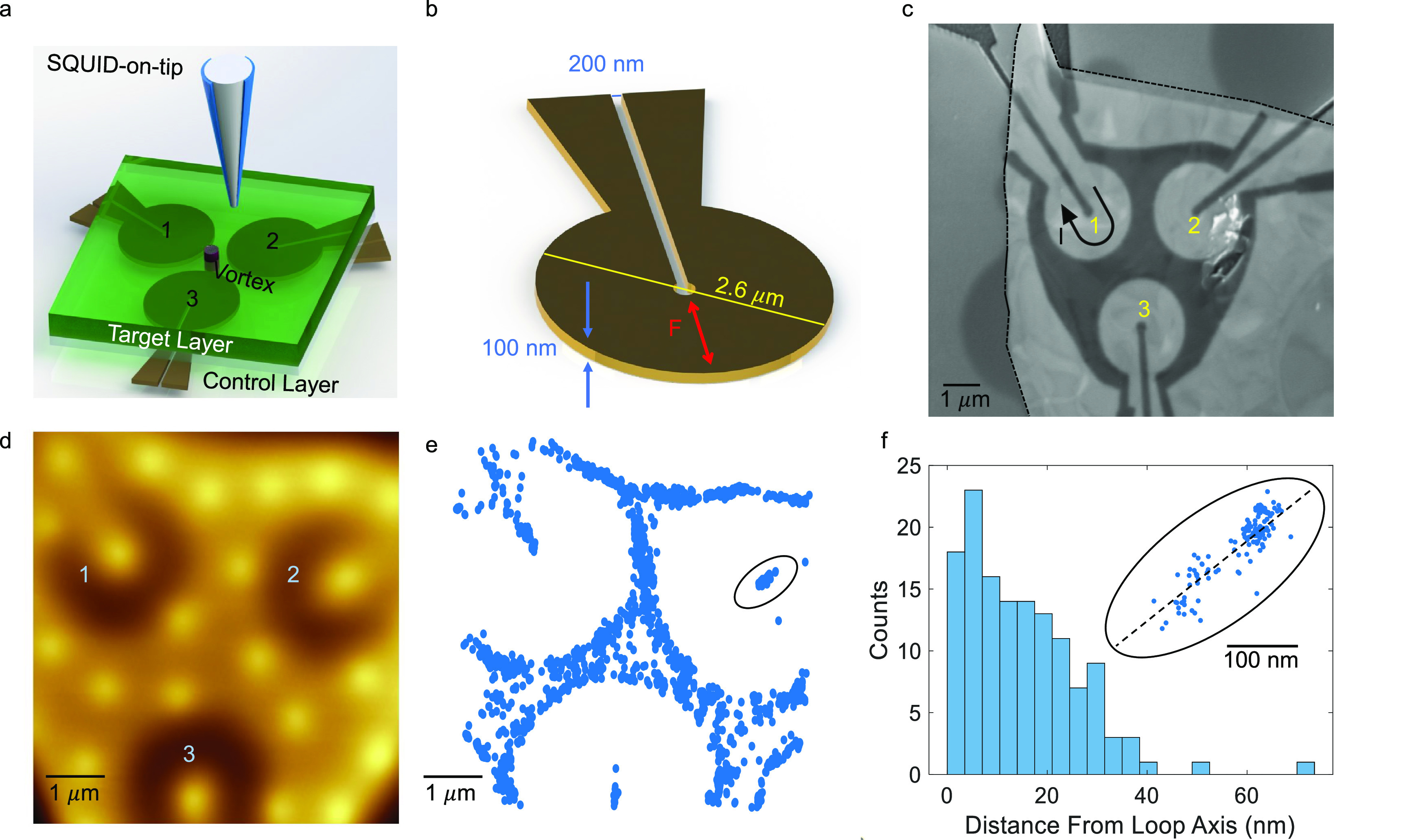
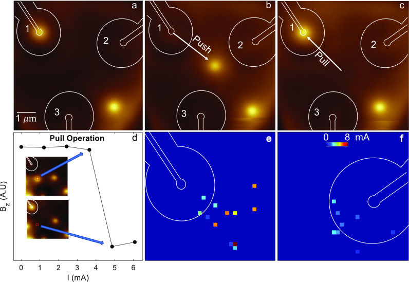
The positions of Abrikosov vortices have long been considered as means to encode classical information. Although it is possible to move individual vortices using local probes, the challenge of scalable on-chip vortex-control remains outstanding, especially when considering the demands of controlling multiple vortices. Realization of vortex logic requires means to shuttle vortices reliably between engineered pinning potentials, while concomitantly keeping all other vortices fixed. We demonstrate such capabilities using Nb loops patterned below a NbSe2 layer. SQUID-on-Tip (SOT) microscopy reveals that the loops localize vortices in designated sites to a precision better than 100 nm; they realize "push" and "pull" operations of vortices as far as 3 μm. Successive application of such operations shuttles a vortex between adjacent loops. Our results may be used as means to integrate vortices in future quantum circuitry. Strikingly, we demonstrate a winding operation, paving the way for future topological quantum computing and simulations.

Keywords: Braiding; Scanning SQUID-on-Tip Microscopy; Topological Quantum Computation; Vortex Manipulation.


Conflict of interest statement

The authors declare no competing financial interest.

Figures

Figure 1
Figure 1
Device parameters. (a) Schematic drawing of the device. The Nb loops (gold) that are etched in the control layer are separated from a ∼50 nm thick NbSe2 target layer (green) by a ∼15 nm thick Al2O3 layer (transparent). A vortex is illustrated within the target layer (purple cylinder). The SQUID-on-tip (SOT) probe is represented above the device as it images the device. (b) Loop geometry. The inner diameter is 200 nm, and the thickness is 100 nm. The outer diameter is 2.6 μm (yellow line). The direction of the total force (F) applied by the loop on the vortex is marked by the red arrow and is parallel to the slit. (c) A top view SEM image of the device. The loops are numbered for future reference. The NbSe2 flake covers all three loops and is highlighted by the black dashed line. The NbSe2 is thin enough to be transparent to the electron beam. The curved arrow indicates the current direction running through Loop 1. (d) Field cooled state with high vortex density. All three loop centers are occupied, each by a single vortex, while no vortices reside overlapping the loop conductor. (e) Compilation of 2370 observed vortices in 500 images. The dots within the black ellipse are used to create the histogram in panel f. (f) Histogram of the points within the black ellipse in panel e. This histogram counts the distances of vortices captured within Loop 2, from the loop axis (dotted black line in the inset where a zoomed in scatter is displayed), resulting in a standard deviation of ∼25 nm.
Figure 2
Figure 2
Basic vortex manipulation. (a) Initial state of the system: Loop 1 is occupied. (b) After passing 2.2 mA through Loop 1, the vortex has escaped out of the loop and is located on a pinning site. (c) After applying −14.6 mA through Loop 1, the vortex was pulled back into the loop. (d) Example of a minimal pull current measurement. The tip position is marked above a specific vortex (red circle). The current through the loop is set to each value and subsequently set to zero. The tip data (local field) is measured (black dots) until the field value drops; a scan verifies that the vortex was indeed pulled into Loop 1. (e) Current map of the minimal current needed to pull vortices from the identified pinning site into Loop 1; the minimal current value increases with distance from the loop center. (f) Same as panel d for Loop 2; the color scale is shared between panels e and f.
Figure 3
Figure 3
Vortex braiding. (a) Initial state of the system after a field cool down using the loop magnetic field. (b) System initialized by pulling Vortex B into Loop 3. Loops 1 and 3 are populated, prepared for the vortex winding operation. Panels b–p are used to create the movie found in the Supporting Information. (c–p) Push and pull operations, circling Vortices A and B around each other. (i) The two vortices have switched positions and have thus been braided. (p) Vortices have completed the full circle around each other, and have thus been wound. The detailed push and pull protocols are described in panel r. Each image is 6 × 6 μm2, contains 128 pixels, and took ∼4 min to acquire. (q) Schematic of the vortices’ full route (A, white; B, yellow). (r) Table listing the operations performed in panels a–q. Each line includes an operation (push/pull), the initial and final locations (e.g., into Loop 3, from the central area), and the panel where the outcome is imaged. Horizontal lines highlight complete shuttle operations, and bold text highlights a complete braiding operation.

References

    1. Reichhardt C. J. O.; Reichhardt C.; Hastings M. B.; Jankó B. Ratchet superconducting vortex cellular automata. Physica C 2004, 404, 266–272. 10.1016/j.physc.2003.11.040. - DOI
    1. Hebard A. F.; Fiory A. T. Memory Device Utilizing the Storage of Abrikosov Vortices At an Array of Pinning Sites in a Superconducting Film. AIP Conf. Proc. 1978, 44, 465–469.
    1. Bachtold W. The Vortex File: A Proposal for A New Application of Type-II Superconductivity. IEEE Trans. Magn. 1979, 15, 558–561. 10.1109/TMAG.1979.1060127. - DOI
    1. Parisi J.; Huebener R. P.; Mühlemeier B. Experimental study of a superconducting vortex-memory device. Appl. Phys. Lett. 1982, 40, 907–909. 10.1063/1.92950. - DOI
    1. Golod T.; Iovan A.; Krasnov V. M. Single Abrikosov vortices as quantized information bits. Nat. Commun. 2015, 6, 8628.10.1038/ncomms9628. - DOI - PMC - PubMed