

Controlling barrier height and spectral responsivity of p-i-n based GeSn photodetectors via arsenic incorporation
- PMID: 36950705
- PMCID: PMC10025945
- DOI: 10.1039/d3ra00805c
Controlling barrier height and spectral responsivity of p-i-n based GeSn photodetectors via arsenic incorporation
Erratum in
-
Correction: Controlling barrier height and spectral responsivity of p-i-n based GeSn photodetectors via arsenic incorporation.RSC Adv. 2023 May 11;13(21):14472. doi: 10.1039/d3ra90040a. eCollection 2023 May 9. RSC Adv. 2023. PMID: 37180013 Free PMC article.
Abstract
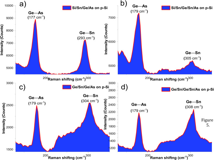
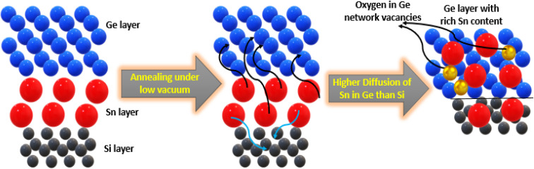
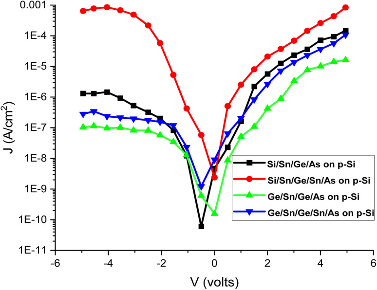
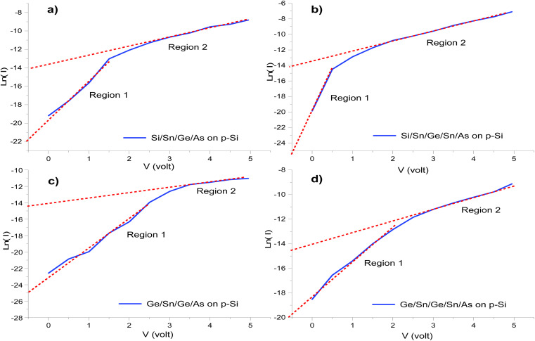
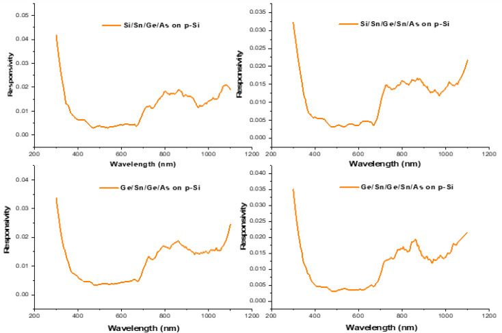
GeSn compounds have made many interesting contributions in photodetectors (PDs) over the last ten years, as they have a detection limit in the NIR and mid-IR region. Sn incorporation in Ge alters the cut off wavelength. In the present article, p-i-n structures based on GeSn junctions were fabricated to serve as PDs. Arsine (As) is incorporated to develop n-GeSn compounds via a metal induced crystallization (MIC) process followed by i-GeSn on p-Si wafers. The impact of As and Sn doping on the strain characteristics of GeSn has been studied with high resolution transmission electron microscopy (HRTEM), X-ray diffraction and Raman spectroscopy analyses. The direct transitions and tuning of their band energies have been investigated using diffuse reflectance UV-vis spectroscopy and photoluminescence (PL). The barrier height and spectral responsivity have been controlled with incorporation of As. Variation of As incorporation into GeSn Compounds shifted the Raman peak and hence affected the strain in the Ge network. UV-vis spectroscopy showed that the direct transition energies are lowered as the Ge-As bonding increases as illustrated in Raman spectroscopy investigations. PL and UV-vis spectroscopy of annealed heterostructures at 500 °C showed that there are many transition peaks from the UV to the NIR region as result of oxygen vacancies in the Ge network. The calculated diode parameters showed that As incorporation leads to an increase of the height barrier and thus dark current. Spectral response measurements show that the prepared heterojunctions have spectral responses in near UV and NIR regions that gives them opportunities in UV and NIR photodetection-applications.
This journal is © The Royal Society of Chemistry.
Conflict of interest statement
The authors declare no competing interests or non-financial interests.
Figures


References
-
- Wang X. Cheng Z. Xu K. Tsang H. K. Xu J. B. High-responsivity graphene/silicon-heterostructure waveguide photodetectors. Nat. Photonics. 2013;7(11):888–891.
-
- Yotter R. A. Wilson D. M. A review of photodetectors for sensing light-emitting reporters in biological systems. IEEE Sens. J. 2003;3(3):288–303.
-
- Soref R. Kouvetakis J. Menendez J. Advances in SiGeSn/Ge technology. MRS Online Proc. Libr. 2006;958:0958-L01.
-
- Barth S. Seifner M. S. Maldonado S. Metastable group IV allotropes and solid solutions: nanoparticles and nanowires. Chem. Mater. 2020;32(7):2703–2741.
LinkOut - more resources
Full Text Sources
Research Materials
Miscellaneous