. 2023 Mar;10(2):023502.
doi: 10.1117/1.JMI.10.2.023502. Epub 2023 Mar 23.

Timing resolution in double-sided silicon photon-counting computed tomography detectors

Affiliations

Timing resolution in double-sided silicon photon-counting computed tomography detectors

Christel Sundberg et al. J Med Imaging (Bellingham). 2023 Mar.

Abstract

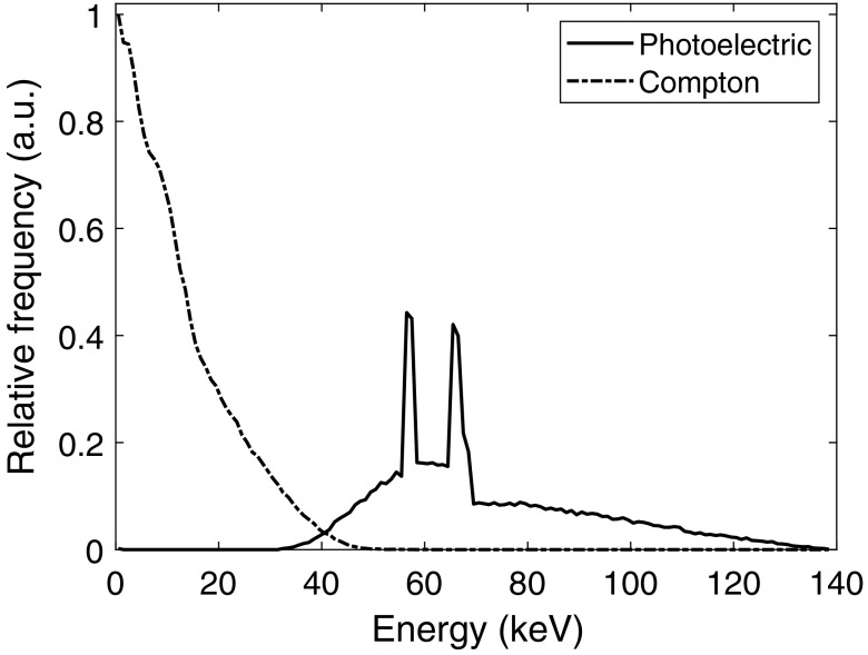
Purpose: Our purpose is to investigate the timing resolution in edge-on silicon strip detectors for photon-counting spectral computed tomography. Today, the timing for detection of individual x-rays is not measured, but in the future, timing information can be valuable to accurately reconstruct the interactions caused by each primary photon.
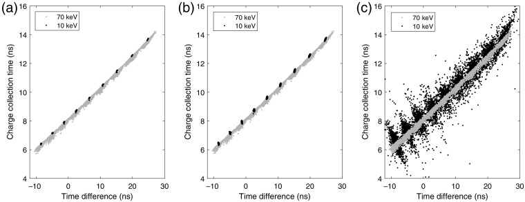
Approach: We assume a pixel size of 12 × 500 μ m 2 and a detector with double-sided readout with low-noise CMOS electronics for pulse processing for every pixel on each side. Due to the electrode width in relation to the wafer thickness, the induced current signals are largely dominated by charge movement close to the collecting electrodes. By employing double-sided readout electrodes, at least two signals are generated for each interaction. By comparing the timing of the induced current pulses, the time of the interaction can be determined and used to identify interactions that originate from the same incident photon. Using a Monte Carlo simulation of photon interactions in combination with a charge transport model, we evaluate the performance of estimating the time of the interaction for different interaction positions.

Results: Our simulations indicate that a time resolution of 1 ns can be achieved with a noise level of 0.5 keV. In a detector with no electronic noise, the corresponding time resolution is 0.1 ns .

Conclusions: Time resolution in edge-on silicon strip CT detectors can potentially be used to increase the signal-to-noise-ratio and energy resolution by helping in identifying Compton scattered photons in the detector.

Keywords: coincidence detection; computed tomography; photon-counting; silicon detector; timing resolution.


Figures

Fig. 1
Fig. 1
Spectrum of the deposited energies in a silicon detector corresponding to the energies deposited in primary Compton and photoelectric interactions. The spectrum was simulated based on an x-ray source operated at 140 kVp including 8.48 mm aluminum, 0.8 mm beryllium, and 300 mm soft tissue filtration between the source and the detector. A target material of tungsten at an 8-deg angle was assumed and the IPEM Report 78 on x-ray spectral data was used to obtain the incident x-ray spectrum. For the attenuating materials, the attenuation coefficients were obtained from NIST. The detector response was simulated in PENELOPE based on a 4-cm deep silicon detector in the direction of the incident photons.
Fig. 2
Fig. 2
(a) Simulated detector geometry as seen from the perspective of the x-ray source. The detector consists of a 500-μm thick silicon wafer that is divided into virtual pixels by electrodes located on each side of the detector. Each electrode is 10μm wide and the pixel pitch is 12  μm. The electrodes on both sides of the wafer have the same geometry and orientation. The incident x-rays enter the detector in the negative z direction. An example of released charge carriers is also included. The large black arrows indicate the drift direction of the electrons and holes, respectively. (b) The assumed detector has several separate rows of electrodes in the direction of the incident x-rays. In this work, the length of the electrodes in this direction was not defined and all simulations were performed in the xy-plane, assuming that the electrode size in the z direction is large in relation to the electrode size in the x direction.
Fig. 3
Fig. 3
(a) Electric potential based on a simulated detector with a bias voltage of 200 V applied to the back-side electrodes, here located at Y=500  μm. (b) Weighting potential of the investigated pixel at the back side of the detector based on a 10-μm electrode width and 12-μm pixel pitch. The potential is 1 V at the position of the electrode. For the front-side electrode, the weighting potential is obtained by rotating the presented distribution 180 deg, so that the electrode is located at a y position of 0  μm.
Fig. 4
Fig. 4
Illustration of the CSA at the input of the readout electronics.
Fig. 5
Fig. 5
(a) Simulated induced current signal from an interaction of 10 keV at the center of the pixel in both the x and y directions, i.e., the distance to the front-side electrode is equal to the distance to the back-side electrode. (b) CSA output voltage based on the induced current pulses. The CSA accumulates the charge and represents the induced current with a voltage of more significant magnitude.
Fig. 6
Fig. 6
CSA output voltage along with fitted template curves for the three noise cases based on an interaction of 10 keV. The input currents correspond to an interaction at the pixel center: i.e., equidistant to the electrodes and to the pixel edges in the x direction. (a) Ideal detector with no noise. (b) Noise corresponding to a standard deviation of σ=0.05  keV. (c) Noise corresponding to a standard deviation of σ=0.5  keV. For the two noise cases, it should be noted that the noise levels in keV are given according to the size at the output of the entire readout channel (including filtering) and not at the CSA output.
Fig. 7
Fig. 7
Average time differences between the time estimates of the front-side and back-side induced pulses for interactions of 10 and 70 keV. The positions indicate the interaction position in the y direction and are presented as percentages of the wafer thickness from the front-side electrode. In the x direction, all interactions are located in the pixel middle, i.e., centered on the electrodes. The included error bars indicate the standard deviation of the estimated time differences for each position. The average time differences are based on 1000 realizations for each interaction position and are presented for each of the assumed noise cases. (a, d) Ideal detector with no noise. Noise corresponding to a standard deviation of (b, e) σ=0.05  keV and (c, f) σ=0.5  keV.
Fig. 8
Fig. 8
Average time differences between the time estimates of the front side and back-side induced pulses. (a)–(c) The results for interactions of 10 keV and (d)–(f) interactions of 70 keV. The interaction positions are indicated as percentages of the wafer thickness from the front-side electrode. The two curves in each subfigure show results for two different interaction positions in the x direction: the pixel middle and the pixel edge. The pixel middle data points are the same as in Fig. 7. The included error bars indicate the standard deviation of the estimated time differences for each position. The average time differences are based on 1000 realizations for each interaction position and are presented for each of the assumed noise cases. (a, d) Ideal detector with no noise. Noise corresponding to a standard deviation of (b, e) σ=0.05  keV and (c, f) σ=0.5  keV.
Fig. 9
Fig. 9
Standard deviations of the time differences between the time estimates of the front-side and back-side induced pulses for interactions of 10 and 70 keV. For each energy, curves are presented for all three noise cases as well as for the two positions in the x direction (pixel middle and pixel edge). Each data point corresponds to the standard deviation of 1000 pulse realizations.
Fig. 10
Fig. 10
Charge collection time as a function of the time difference between the time estimates of the front-side and back-side pulses for interactions of 10 and 70 keV. The interactions are centered on the electrodes in the x direction. With an interaction at time t=0, the charge collection time describes the time between the interaction and the average time of the front-side and back-side induced pulse. Each scatter plot shows 9000 realizations (1000 realizations for each of the 9 positions between the front-side and back-side electrodes) for each energy and noise case. (a) Ideal detector with no noise. Noise corresponding to a standard deviation of (b) σ=0.05  keV and (c)σ=0.5  keV.
Fig. 11
Fig. 11
Charge collection time as a function of the time difference between the time estimates of the front-side and back-side pulses for interactions of (a)–(c) 10 keV and (d)–(f) 70 keV. With an interaction at time t=0, the charge collection time describes the time between the interaction and the average time of the front-side and back-side induced pulse. Results are shown for two different interaction positions in the x direction: the pixel middle and the pixel edge. The pixel middle data points are the same as in Fig. 10. Each scatter plot shows 9000 realizations (1000 realizations for each of the 9 positions between the front-side and back-side electrodes) for each energy and noise case. (a, d) Ideal detector with no noise and noise corresponding to a standard deviation of (b, e) σ=0.05  keV and (c, f) σ=0.5  keV. For each position in the x direction, a curve was fitted to the data.

References

    1. da Silva J., et al. , “Resolution characterization of a silicon-based, photon-counting computed tomography prototype capable of patient scanning,” J. Med. Imaging 6, 043502 (2019).JMEIET10.1117/1.JMI.6.4.043502 - DOI - PMC - PubMed
    1. Danielsson M., Persson M., Sjölin M., “Photon-counting x-ray detectors for CT,” Phys. Med. Biol. 66, 03TR01 (2021).10.1088/1361-6560/abc5a5 - DOI - PubMed
    1. Grönberg F., et al. , “Feasibility of unconstrained three-material decomposition: imaging an excised human heart using a prototype silicon photon-counting CT detector,” Eur. Radiol. 30, 5904–5912 (2020).EURAE310.1007/s00330-020-07017-y - DOI - PMC - PubMed
    1. Cranley K., Gilmore B. J., Fogarty G. W. A., “SRS-78: catalogue of diagnostic x-ray spectra and other data,” Tech. Rep., Institute of Physics and Engineering in Medicine, York, UK (1997).
    1. Berger M., et al. , “XCOM: photon cross section database (version 1.5)” (2010).