. 2023 Mar 15;16(6):2344.
doi: 10.3390/ma16062344.

Fully Integrated Silicon Photonic Erbium-Doped Nanodiode for Few Photon Emission at Telecom Wavelengths

Affiliations

Fully Integrated Silicon Photonic Erbium-Doped Nanodiode for Few Photon Emission at Telecom Wavelengths

Giulio Tavani et al. Materials (Basel). .

Abstract

Recent advancements in quantum key distribution (QKD) protocols opened the chance to exploit nonlaser sources for their implementation. A possible solution might consist in erbium-doped light emitting diodes (LEDs), which are able to produce photons in the third communication window, with a wavelength around 1550 nm. Here, we present silicon LEDs based on the electroluminescence of Er:O complexes in Si. Such sources are fabricated with a fully-compatible CMOS process on a 220 nm-thick silicon-on-insulator (SOI) wafer, the common standard in silicon photonics. The implantation depth is tuned to match the center of the silicon layer. The erbium and oxygen co-doping ratio is tuned to optimize the electroluminescence signal. We fabricate a batch of Er:O diodes with surface areas ranging from 1 µm × 1 µm to 50 µm × 50 µm emitting 1550 nm photons at room temperature. We demonstrate emission rates around 5 × 10⁶ photons/s for a 1 µm × 1 µm device at room temperature using superconducting nanowire detectors cooled at 0.8 K. The demonstration of Er:O diodes integrated in the 220 nm SOI platform paves the way towards the creation of integrated silicon photon sources suitable for arbitrary-statistic-tolerant QKD protocols.

Keywords: SOI diode; erbium doping; quantum key distribution; silicon photonics.


Conflict of interest statement

The authors declare no conflict of interest.

Figures

Figure 1
Figure 1
(a) Silicon on insulator wafer, the silicon layer is 220 nm-thick and it lies on a 3 µm-thick SiO2 buried layer. (b) Mesa of the device defined by electron beam lithography (30 keV) using a positive resist (PMMA). The etching is performed via a Bosch process. (c) Sketch illustrating the doping of the device. In red, the p-area doped with boron, in blue, the one doped with phosphorous, and, in green, the region co-doped with erbium and oxygen. (d) Final device. In yellow, the electrical contacts made of titanium and gold. (e) Scanning electron microscopy image of the device. Our simulations indicate that most of the photons are confined in the silicon layer and just 6% of them are emitted in open space in the vertical direction. (f) Energy level structure in Er3+, the transition exploited in our device is displayed.
Figure 2
Figure 2
(a) Layout of the device simulated with FDTD. In red, the optically active part of the device is represented. This is simulated as a 1 µm × 1 µm undoped silicon square with dipole sources in it. The silicon oxide layer is the grey box and the contacts (in blue) are modelled as doped silicon regions. The blue arrow indicates the orientation of the dipole source whereas the grey concentric lines are the dipole radiation pattern. (b) Modification of the Purcell factor considering a variation of the lateral size of the optically active area.
Figure 3
Figure 3
Photoluminescence spectra recorded for three different oxygen co-doping doses. On the left, samples are annealed for 30 min at a temperature TAnn = 900 °C. On the right, the annealing is performed at 920 °C for the same amount of time. All the signals are normalized with respect to the PL maximum obtained with a dose equals to 1.4 × 1014 O cm2 and the annealing temperature equals to 900 °C.
Figure 4
Figure 4
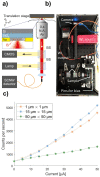
(a) Sketch of the experimental setup. (b) Picture of the the experimental setup (top view). (c) Counts collected per second in each device as a function of the current flux measured on the diode.

References

    1. Cavaliere F., Prati E., Poti L., Muhammad I., Catuogno T. Secure quantum communication technologies and systems: From labs to markets. Quant. Rep. 2020;2:80–106. doi: 10.3390/quantum2010007. - DOI
    1. Lo H.K., Ma X., Chen K. Decoy state quantum key distribution. Phys. Rev. Lett. 2005;94:230504. doi: 10.1103/PhysRevLett.94.230504. - DOI - PubMed
    1. Sibson P., Kennard J.E., Stanisic S., Erven C., O’Brien J.L., Thompson M.G. Integrated silicon photonics for high-speed quantum key distribution. Optica. 2017;4:172–177. doi: 10.1364/OPTICA.4.000172. - DOI
    1. Tran T.N.L., Berneschi S., Trono C., Conti G.N., Zur L., Armellini C., Varas S., Carpentiero A., Chiappini A., Chiasera A., et al. SiO2-SnO2: Er3+ planar waveguides: Highly photorefractive glass-ceramics. Opt. Mater. 2020;7:100056. doi: 10.1016/j.omx.2020.100056. - DOI
    1. Agnesi C., Da Lio B., Cozzolino D., Cardi L., Bakir B.B., Hassan K., Della Frera A., Ruggeri A., Giudice A., Vallone G., et al. Hong–Ou–Mandel interference between independent III–V on silicon waveguide integrated lasers. Opt. Lett. 2019;44:271–274. doi: 10.1364/OL.44.000271. - DOI - PubMed