. 2023 Mar 22;13(6):1134.
doi: 10.3390/nano13061134.

The Effect of C60 and Pentacene Adsorbates on the Electrical Properties of CVD Graphene on SiO2

Affiliations

The Effect of C60 and Pentacene Adsorbates on the Electrical Properties of CVD Graphene on SiO2

Jacopo Oswald et al. Nanomaterials (Basel). .

Abstract

Graphene is an excellent 2D material for vertical organic transistors electrodes due to its weak electrostatic screening and field-tunable work function, in addition to its high conductivity, flexibility and optical transparency. Nevertheless, the interaction between graphene and other carbon-based materials, including small organic molecules, can affect the graphene electrical properties and therefore, the device performances. This work investigates the effects of thermally evaporated C60 (n-type) and Pentacene (p-type) thin films on the in-plane charge transport properties of large area CVD graphene under vacuum. This study was performed on a population of 300 graphene field effect transistors. The output characteristic of the transistors revealed that a C60 thin film adsorbate increased the graphene hole density by (1.65 ± 0.36) × 1012 cm-2, whereas a Pentacene thin film increased the graphene electron density by (0.55 ± 0.54) × 1012 cm-2. Hence, C60 induced a graphene Fermi energy downshift of about 100 meV, while Pentacene induced a Fermi energy upshift of about 120 meV. In both cases, the increase in charge carriers was accompanied by a reduced charge mobility, which resulted in a larger graphene sheet resistance of about 3 kΩ at the Dirac point. Interestingly, the contact resistance, which varied in the range 200 Ω-1 kΩ, was not significantly affected by the deposition of the organic molecules.

Keywords: C60; Pentacene; field effect; graphene; heterostructures; hybrid; organic; semiconductor; transistor; van der Waals.


Conflict of interest statement

The authors declare no conflict of interest.

Figures

Figure 1
Figure 1
(a) Optical microscope image of a representative Graphene Field Effect Transistor (GFET). The channel length L and width W of this device are 50 μm and 5 μm, respectively. The image shows the source (S) and drain (D) gold electrodes on the Si/SiO2 substrate. (b) Electrical schematic of the GFET (not to scale). The cross-section shows the heavily p-doped Si Gate (G), the SiO2 dielectric (300 nm), the Ti/Au source/drain (5 nm/50 nm) and the Gr channel coated with C60 or Pentacene molecules. The source (S) electrode is connected to ground. In the gate-to-source voltage (VGS) sweep, the drain-to-source bias (VDS) is kept constant while the current (IDS) is measured. (c) Energetic representation of the Highest Occupied Molecular Orbital (HOMO) and Lowest Unoccupied Molecular Orbital (LUMO) nominal levels of the C60 and Pentacene molecules with respect to the Fermi energy level of pristine graphene (black dashed line). The Fermi energy of graphene lies within 0.5 eV from the HOMO energy level of Pentacene and within 0.5 eV from LUMO energy level of C60.
Figure 2
Figure 2
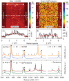
Surface morphology and chemical composition of the Gr/C60 (Chip 1) and Gr/Pentacene (Chip 2) heterostructures. (a) AFM height image of a representative Gr/C60 FET channel. (b) AFM height image of a representative Gr/Pentacene FET channel. (c) AFM height profile (black line) of the Gr/C60 FET channel taken along the dashed white line in (a). The red line is the mean value of 128 height profiles shown by the white bars in the AFM image. (d) AFM height profile (black line) of the Gr/Pentacene FET channel taken along the dashed white line in (b). The red line is the mean value of 128 height profiles shown by the white bars in the AFM image. (e) Average Raman spectra of the C60-GFETs (Chip 1). The Raman spectrum of the pristine CVD graphene is blue, while the Raman spectrum of Gr/C60 is orange. (f) Average Raman spectra of the Pentacene-GFETs (Chip 2). The Raman spectrum of the pristine CVD graphene is green, while the Raman spectrum of Gr/Pentacene is red. All spectra are normalized to the 2D peak of graphene. The triangle, square, circle and star symbols represent the characteristic Raman peaks of Si [34], Gr [33], C60 [35] and Pentacene [32], respectively.
Figure 3
Figure 3
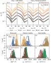
GFETs’ electrical measurements. (a) Average transfer characteristic (IDS vs. VGS) of pristine CVD graphene FETs before C60 deposition (Chip 1, 101 devices, all L included). The shaded areas are the standard deviations. (b) Average transfer characteristic of the C60-GFETs (Chip 1, 101 devices, all L included). (c) Average transfer characteristic of pristine CVD graphene before Pentacene deposition (Chip 2, 119 devices, all L included). (d) Average transfer characteristic of the Pentacene-GFETs (Chip 2, 98 devices, all L included). (e) Histograms of the graphene Dirac position (VGSDirac) before (blue) and after deposition of C60 (orange). (f) Histograms of the graphene electron mobility (μe) before (blue) and after deposition of C60 (orange), all L included. (g) Histograms of the graphene hole mobility (μh) before (blue) and after deposition of C60 (orange), all L included. (h) Histograms of the graphene Dirac position (VGSDirac) before (green) and after deposition of Pentacene (red), all L included. (i) Histograms of the graphene electron mobility (μe) before (green) and after deposition of Pentacene (red), all L included. (j) Histograms of the graphene hole mobility (μh) before (green) and after deposition of Pentacene (red), all L included. Bins width of graphene Dirac point position and mobility histograms are 2 V and 100 cm2V−1s−1, respectively.
Figure 4
Figure 4
GFETs’ sheet resistance (RS) and contact resistance (RC) represented by solid and dashed lines, respectively. (a) RS (solid line) and RC (dashed line) of pristine CVD graphene before (blue) and after (orange) deposition of C60 (Chip 1). The circles and triangles show the maxima and minima of the contact resistance, respectively. The arrows show the shift of the maximum of RS and of the maximum of RC due to the deposition of the molecules. (b) RS (solid line) and RC (dashed line) of pristine CVD graphene before (green) and after (red) deposition of Pentacene (Chip 2). The shaded areas are the standard errors of the estimated slope and intercept of the linear regression method used to extrapolate RS and RC with the Transfer Length Method (TLM) from the datasets presented in Figure 3a–d. (c) Schematic of the residual p-doping of graphene due to C60 deposition (Chip 1). (d) Schematic of the residual n-doping of graphene due to Pentacene deposition (Chip 2).

References

    1. Huisman E.H., Shulga A.G., Zomer P.J., Tombros N., Bartesaghi D., Bisri S.Z., Loi M.A., Koster L.J.A., Van Wees B.J. High Gain Hybrid Graphene–Organic Semiconductor Phototransistors. ACS Appl. Mater. Interfaces. 2015;7:11083–11088. doi: 10.1021/acsami.5b00610. - DOI - PubMed
    1. Shangguan Q., Chen Z., Yang H., Cheng S., Yang W., Yi Z., Wu X., Wang S., Yi Y., Wu P. Design of Ultra-Narrow Band Graphene Refractive Index Sensor. Sensors. 2022;22:6483. doi: 10.3390/s22176483. - DOI - PMC - PubMed
    1. Garg R., Elmas S., Nann T., Andersson M.R. Deposition Methods of Graphene as Electrode Material for Organic Solar Cells. Adv. Energy Mater. 2017;7:1601393. doi: 10.1002/aenm.201601393. - DOI
    1. Adetayo A.E., Ahmed T.N., Zakhidov A., Beall G.W. Improvements of Organic Light-Emitting Diodes Using Graphene as an Emerging and Efficient Transparent Conducting Electrode Material. Adv. Opt. Mater. 2021;9:2002102. doi: 10.1002/adom.202002102. - DOI
    1. Liu L., Liu Y., Duan X. Graphene-Based Vertical Thin Film Transistors. Sci. China Inf. Sci. 2020;63:201401. doi: 10.1007/s11432-020-2806-8. - DOI

LinkOut - more resources