Continuous Large Area Monolayered Molybdenum Disulfide Growth Using Atmospheric Pressure Chemical Vapor Deposition
- PMID: 37008105
- PMCID: PMC10061614
- DOI: 10.1021/acsomega.2c07408
Continuous Large Area Monolayered Molybdenum Disulfide Growth Using Atmospheric Pressure Chemical Vapor Deposition
Abstract
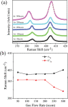
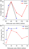
The growth of large crystallite continuous monolayer materials like molybdenum disulfide (MoS2) with the desired morphology via chemical vapor deposition (CVD) remains a challenge. In CVD, the complex interplay of various factors like growth temperatures, precursors, and nature of the substrate decides the crystallinity, crystallite size, and coverage area of the grown MoS2 monolayer. In the present work, we report about the role of weight fraction of molybdenum trioxide (MoO3), sulfur, and carrier gas flow rate toward nucleation and monolayer growth. The concentration of MoO3 weight fraction has been found to govern the self-seeding process and decides the density of nucleation sites affecting the morphology and coverage area. A carrier gas flow of 100 sccm argon results in large crystallite continuous films with a lower coverage area (70%), while a flow rate of 150 sccm results in 92% coverage area with a reduced crystallite size. Through a systematic variation of experimental parameters, we have established the recipe for the growth of large crystallite atomically thin MoS2 suitable for optoelectronic devices.
© 2023 The Authors. Published by American Chemical Society.
Conflict of interest statement
The authors declare no competing financial interest.
Figures



Similar articles
-
Influence of the Carrier Gas Flow in the CVD Synthesis of 2-Dimensional MoS2 Based on the Spin-Coating of Liquid Molybdenum Precursors.Nanomaterials (Basel). 2024 Oct 31;14(21):1749. doi: 10.3390/nano14211749. Nanomaterials (Basel). 2024. PMID: 39513829 Free PMC article.
-
Control of the Nucleation Density of Molybdenum Disulfide in Large-Scale Synthesis Using Chemical Vapor Deposition.Materials (Basel). 2018 May 23;11(6):870. doi: 10.3390/ma11060870. Materials (Basel). 2018. PMID: 29882847 Free PMC article.
-
Application-Oriented Growth of a Molybdenum Disulfide (MoS2) Single Layer by Means of Parametrically Optimized Chemical Vapor Deposition.Materials (Basel). 2020 Jun 20;13(12):2786. doi: 10.3390/ma13122786. Materials (Basel). 2020. PMID: 32575719 Free PMC article.
-
Uniform Vapor-Pressure-Based Chemical Vapor Deposition Growth of MoS2 Using MoO3 Thin Film as a Precursor for Coevaporation.ACS Omega. 2018 Dec 31;3(12):18943-18949. doi: 10.1021/acsomega.8b02978. eCollection 2018 Dec 31. ACS Omega. 2018. PMID: 31458458 Free PMC article.
-
Comparative Study between Sulfurized MoS2 from Molybdenum and Molybdenum Trioxide Precursors for Thin-Film Device Applications.ACS Appl Mater Interfaces. 2023 Mar 29;15(12):16308-16316. doi: 10.1021/acsami.3c00824. Epub 2023 Mar 20. ACS Appl Mater Interfaces. 2023. PMID: 36939015
Cited by
-
Highly Stable Electronics Based on β-Ga2O3 for Advanced Memory Applications.Adv Sci (Weinh). 2025 Mar;12(12):e2413846. doi: 10.1002/advs.202413846. Epub 2025 Feb 5. Adv Sci (Weinh). 2025. PMID: 39910929 Free PMC article.
-
CVD Synthesis of MoS2 Using a Direct MoO2 Precursor: A Study on the Effects of Growth Temperature on Precursor Diffusion and Morphology Evolutions.Materials (Basel). 2023 Jul 4;16(13):4817. doi: 10.3390/ma16134817. Materials (Basel). 2023. PMID: 37445130 Free PMC article.
References
-
- Balendhran S.; Walia S.; Nili H.; Ou J. Z.; Zhuiykov S.; Kaner R. B.; Sriram S.; Bhaskaran M.; Kalantar-zadeh K. Two-dimensional molybdenum trioxide and dichalcogenides. Adv. Funct. Mater. 2013, 23, 3952–3970. 10.1002/adfm.201300125. - DOI
LinkOut - more resources
Full Text Sources

