. 2023 Apr 3;12(1):84.
doi: 10.1038/s41377-023-01128-z.

Monolithic integration of embedded III-V lasers on SOI

Affiliations

Monolithic integration of embedded III-V lasers on SOI

Wen-Qi Wei et al. Light Sci Appl. .

Abstract

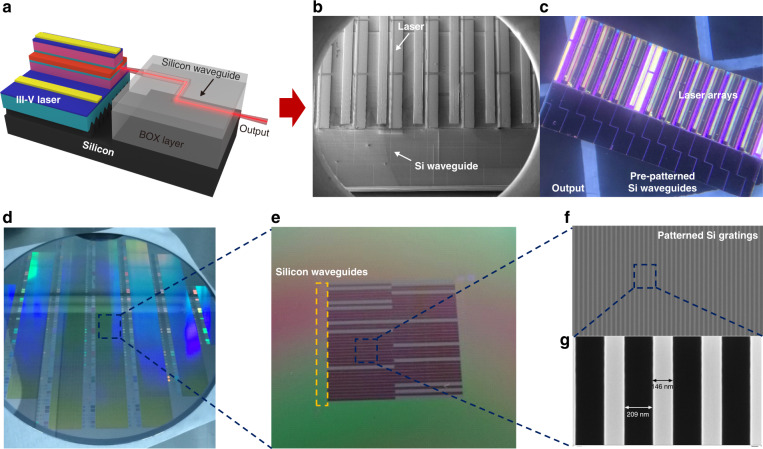
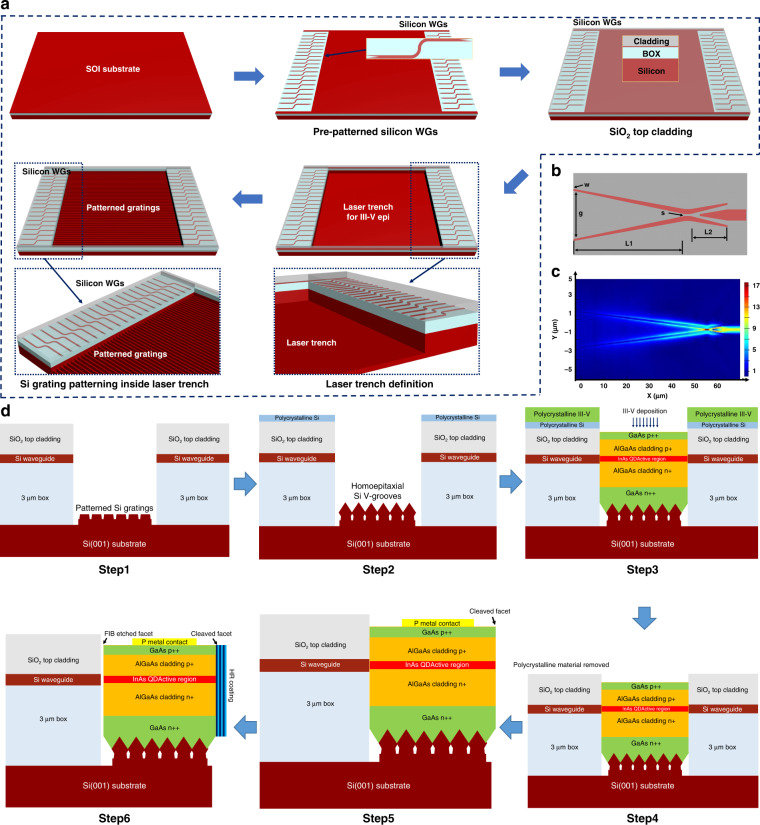
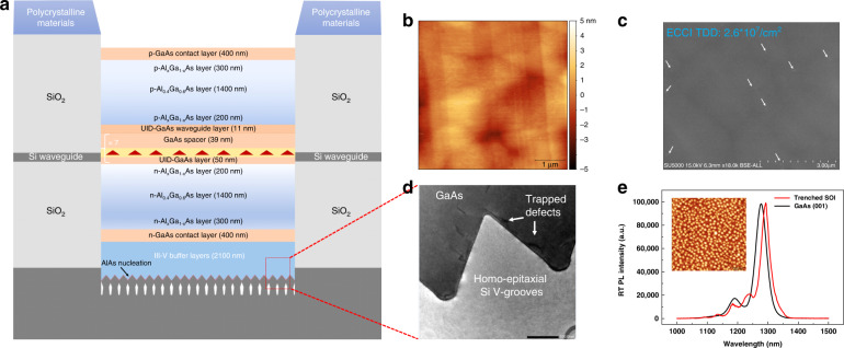
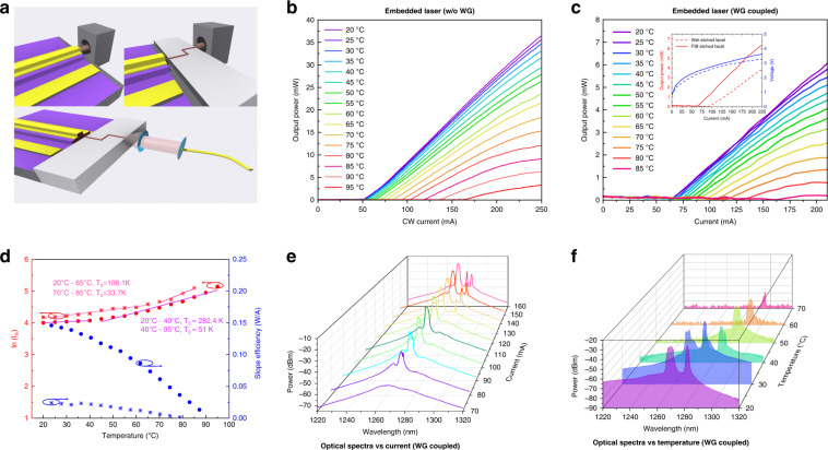
Silicon photonic integration has gained great success in many application fields owing to the excellent optical device properties and complementary metal-oxide semiconductor (CMOS) compatibility. Realizing monolithic integration of III-V lasers and silicon photonic components on single silicon wafer is recognized as a long-standing obstacle for ultra-dense photonic integration, which can provide considerable economical, energy-efficient and foundry-scalable on-chip light sources, that has not been reported yet. Here, we demonstrate embedded InAs/GaAs quantum dot (QD) lasers directly grown on trenched silicon-on-insulator (SOI) substrate, enabling monolithic integration with butt-coupled silicon waveguides. By utilizing the patterned grating structures inside pre-defined SOI trenches and unique epitaxial method via hybrid molecular beam epitaxy (MBE), high-performance embedded InAs QD lasers with monolithically out-coupled silicon waveguide are achieved on such template. By resolving the epitaxy and fabrication challenges in such monolithic integrated architecture, embedded III-V lasers on SOI with continuous-wave lasing up to 85 °C are obtained. The maximum output power of 6.8 mW can be measured from the end tip of the butt-coupled silicon waveguides, with estimated coupling efficiency of approximately -6.7 dB. The results presented here provide a scalable and low-cost epitaxial method for the realization of on-chip light sources directly coupling to the silicon photonic components for future high-density photonic integration.


Conflict of interest statement

The authors declare no competing interests.

Figures

Fig. 1
Fig. 1. Monolithically integrated embedded InAs QD lasers on SOI characterizations in this work.
a Schematic of monolithic integration of III-V QD laser edge coupled with silicon waveguide on SOI platform. b Top-view SEM image of InAs QD laser arrays grown in pre-patterned laser trenches, with passive silicon WGs. c Optical microscope image of entire integrated chip. d 8-inch SOI wafer with pre-patterned laser trenches and silicon waveguides. e Zoomed-in optical microscope image of laser trenches with aligned silicon waveguide arrays on SOI substrate. f Top-view SEM image of patterned silicon grating structures inside laser trenches for III-V growth. g Magnified silicon gratings with slab width of 146 nm and gap width of 209 nm. The duty cycle of this grating is approximately 40% inside the laser trench
Fig. 2
Fig. 2. Schematic diagram of patterned SOI trenches and design of edge coupler.
a Fabrication flows of patterned SOI template with 3 μm BOX layer and 220 nm top Si layer. b The layout and parameters of silicon fork coupler. c Electric field distribution of the edge coupler. d Schematic diagram of embedded laser process on trenched SOI. Step 1: The exposed silicon substrate patterned with silicon gratings. Step 2: Homoepitaxially formed Si V-groove structures over the top of silicon gratings. Step 3: InAs/GaAs QD laser epi-structures directly grown inside the SOI trench. Step 4: Chemical remove of unwanted III-V materials outside the SOI trench. Step 5: Fabricated narrow ridge laser with one-side as-cleaved facets. Step 6: Final embedded QD lasers with direct edge coupling into pre-patterned silicon waveguides
Fig. 3
Fig. 3. Epitaxial growth structures and material characterization.
a Schematic of the laser epi-structures. b Surface AFM image of 2100 nm thick III-V buffer layers grown on trenched SOI before epitaxial growth of laser sturctures (RMS ~ 0.8 nm). c TDD estimated from ECCI image (2.6 ×10⁷ /cm2). d Cross-sectional TEM image of as-grown GaAs/Si interface on trenched region of SOI substrate. e PL spectra comparison between InAs QDs grown on trenched SOI substrate and standard GaAs substrate under identical conditions. Inset: AFM image of surface InAs QDs on trenched SOI
Fig. 4
Fig. 4. Fabricated monolithically integrated InAs QD lasers coupled to silicon waveguides.
a Tilted SEM image of entire integrated chip. b SEM image of fabricated narrow ridge laser directly coupled with silicon waveguides using fork-like mode converter. c SEM image of silicon waveguide mode converter. d Magnified SEM image of single embedded laser edge-coupled with silicon waveguide. e Optical microscope of monolithically integrated laser and silicon WG. f SEM images of the embedded lasers with wet etched and FIB etched facets, respectively. g White light interferometric image of the finalized devices
Fig. 5
Fig. 5. Continuous-wave characterizations of embedded InAs QD laser on SOI with and without coupling into silicon waveguide.
a Schematics of L-I and optical spectral measurements; top left: L-I measurements of double-side cleaved III-V laser inside SOI trench; top right: L-I measurements of embedded InAs QD laser from silicon waveguide output; bottom: optical spectral measurements from the silicon waveguide. b Continuous-wave temperature-dependent L-I measurements of double-side cleaved III-V laser inside SOI trench as reference laser. c Continuous-wave temperature-dependent L-I measurements of integrated laser with one cleaved facet and FIB etched for the other; inset: room-temperature L-I comparison between single-side wet etched facet and FIB etched facet. d Plots of natural logarithm of threshold current and slope efficiency versus varied operating temperatures; characteristic temperature (To) are fitted for double-side cleaved embedded laser (red dots) in temperature ranges from 20 to 40 °C and 45 to 95 °C, respectively; characteristic temperature (To) are fitted for embedded laser with integrated silicon WG (red stars) in temperature ranges from 20 to 65 °C and 70 to 85 °C, respectively. e Optical spectral analysis of integrated laser versus increased injection current. f Optical spectral analysis of integrated laser versus temperature variation

Similar articles

Cited by

References

    1. Miller DAB. Device requirements for optical interconnects to silicon chips. Proc. IEEE. 2009;97:1166–1185. doi: 10.1109/JPROC.2009.2014298. - DOI
    1. Asghari M, Krishnamoorthy AV. Silicon photonics: energy-efficient communication. Nat. Photo. 2011;5:268–270. doi: 10.1038/nphoton.2011.68. - DOI
    1. Rickman A. The commercialization of silicon photonics. Nat. Photonics. 2014;8:579–582. doi: 10.1038/nphoton.2014.175. - DOI
    1. Komljenovic T, et al. Photonic integrated circuits using heterogeneous integration on silicon. Proc. IEEE. 2018;106:2246–2257. doi: 10.1109/JPROC.2018.2864668. - DOI
    1. Zhou ZP, Yin B, Michel J. On-chip light sources for silicon photonics. Light Sci. Appl. 2015;4:e358. doi: 10.1038/lsa.2015.131. - DOI - PMC - PubMed