Monolithic integration of embedded III-V lasers on SOI
- PMID: 37009809
- PMCID: PMC10068801
- DOI: 10.1038/s41377-023-01128-z
Monolithic integration of embedded III-V lasers on SOI
Abstract
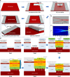
Silicon photonic integration has gained great success in many application fields owing to the excellent optical device properties and complementary metal-oxide semiconductor (CMOS) compatibility. Realizing monolithic integration of III-V lasers and silicon photonic components on single silicon wafer is recognized as a long-standing obstacle for ultra-dense photonic integration, which can provide considerable economical, energy-efficient and foundry-scalable on-chip light sources, that has not been reported yet. Here, we demonstrate embedded InAs/GaAs quantum dot (QD) lasers directly grown on trenched silicon-on-insulator (SOI) substrate, enabling monolithic integration with butt-coupled silicon waveguides. By utilizing the patterned grating structures inside pre-defined SOI trenches and unique epitaxial method via hybrid molecular beam epitaxy (MBE), high-performance embedded InAs QD lasers with monolithically out-coupled silicon waveguide are achieved on such template. By resolving the epitaxy and fabrication challenges in such monolithic integrated architecture, embedded III-V lasers on SOI with continuous-wave lasing up to 85 °C are obtained. The maximum output power of 6.8 mW can be measured from the end tip of the butt-coupled silicon waveguides, with estimated coupling efficiency of approximately -6.7 dB. The results presented here provide a scalable and low-cost epitaxial method for the realization of on-chip light sources directly coupling to the silicon photonic components for future high-density photonic integration.
© 2023. The Author(s).
Conflict of interest statement
The authors declare no competing interests.
Figures


References
-
- Miller DAB. Device requirements for optical interconnects to silicon chips. Proc. IEEE. 2009;97:1166–1185. doi: 10.1109/JPROC.2009.2014298. - DOI
-
- Asghari M, Krishnamoorthy AV. Silicon photonics: energy-efficient communication. Nat. Photo. 2011;5:268–270. doi: 10.1038/nphoton.2011.68. - DOI
-
- Rickman A. The commercialization of silicon photonics. Nat. Photonics. 2014;8:579–582. doi: 10.1038/nphoton.2014.175. - DOI
-
- Komljenovic T, et al. Photonic integrated circuits using heterogeneous integration on silicon. Proc. IEEE. 2018;106:2246–2257. doi: 10.1109/JPROC.2018.2864668. - DOI
Grants and funding
- 2021YFB2800403/Ministry of Science and Technology of the People's Republic of China (Chinese Ministry of Science and Technology)
- Y2022005/Youth Innovation Promotion Association of the Chinese Academy of Sciences (Youth Innovation Promotion Association CAS)
- 61975230,62225407,62008308/National Natural Science Foundation of China (National Science Foundation of China)
LinkOut - more resources
Full Text Sources
Miscellaneous

