. 2023 May;617(7959):67-72.
doi: 10.1038/s41586-023-05848-5. Epub 2023 Apr 5.

Two-dimensional ferroelectricity in a single-element bismuth monolayer

Affiliations

Two-dimensional ferroelectricity in a single-element bismuth monolayer

Jian Gou et al. Nature. 2023 May.

Abstract

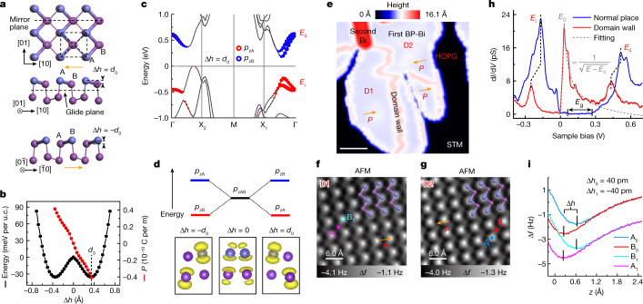
Ferroelectric materials are fascinating for their non-volatile switchable electric polarizations induced by the spontaneous inversion-symmetry breaking. However, in all of the conventional ferroelectric compounds, at least two constituent ions are required to support the polarization switching1,2. Here, we report the observation of a single-element ferroelectric state in a black phosphorus-like bismuth layer3, in which the ordered charge transfer and the regular atom distortion between sublattices happen simultaneously. Instead of a homogenous orbital configuration that ordinarily occurs in elementary substances, we found the Bi atoms in a black phosphorous-like Bi monolayer maintain a weak and anisotropic sp orbital hybridization, giving rise to the inversion-symmetry-broken buckled structure accompanied with charge redistribution in the unit cell. As a result, the in-plane electric polarization emerges in the Bi monolayer. Using the in-plane electric field produced by scanning probe microscopy, ferroelectric switching is further visualized experimentally. Owing to the conjugative locking between the charge transfer and atom displacement, we also observe the anomalous electric potential profile at the 180° tail-to-tail domain wall induced by competition between the electronic structure and electric polarization. This emergent single-element ferroelectricity broadens the mechanism of ferroelectrics and may enrich the applications of ferroelectronics in the future.


Conflict of interest statement

The authors declare no competing interests.

Figures

Fig. 1
Fig. 1. Non-centrosymmetric structure of BP-Bi.
a, Schematic lattice structure of single layer BP-Bi. Top and side views of Δh = d0 state are shown in the top and middle panels, respectively. For the Δh = −d0 state, only a side-view model is shown in the bottom panel. The topmost Bi atoms are coloured light blue to only guide the eye for a better comparison with AFM images. b, Calculated free energy per unit cell (u.c.) and polarization P versus the buckling Δh show an anharmonic double-well potential and nearly linear relation, respectively. c, Band structure of BP-Bi when Δh adopts the right minimum (d0) of the double-well potential in b. The size of the red (blue) circles represents the contributions of the pz orbital of sublattice A(B). d, Illustration of the revolution of pz orbitals at sublattice A and B (top panel). Projected pz valence charge density corresponding to three buckling conditions (Δh = −d0, Δh = 0, Δh = d0) are shown in the bottom panel. e, STM image of BP-Bi on HOPG (V = 0.2 V, I = 10 pA). Scale bar, 10 nm. f,g, AFM images of two domains (D1 (f) and D2 (g)). Ball-and-stick models of the top two layers are superimposed to highlight the atom position. h, dI/dV measured at the domain area and a domain wall (head-to-head, V = 0.7 V, I = 1.2 nA). The density-of-states (DOS) maximum corresponding to the pz bands at Γ point is labelled as Ei and Eii. i, Δf(z) spectra measured on the two sublatticed in f and g. A0 and B0 are up-shifted by 2 Hz for clarity. Vertical short bars mark the turn points of the Δf(z) curves. Tip height z = −260 pm (f,g,i) relative to the height determined by the setpoint V = 100 mV, I = 10 pA above the BP-Bi surface.
Fig. 2
Fig. 2. Electron redistribution at A and B sublattice of monolayer BP-Bi.
a, AFM image of a monolayer BP-Bi. Red and blue dotted circles highlight two atoms in the two sublattices. Scale bar, 4.0 Å. b, Constant-height dI/dV spectra obtained along the red dashed arrow in a. c,d, Constant-height dI/dV mapping of the occupied states (c) and empty states (d) in the same area as a. e, Typical frequency shift (Δf) curve as a function of sample bias is measured above the Bi atoms at the constant-height mode (black circles). Red parabolic fitting (red solid line) yields the V* at the maximum to represent the LCPD. The inset shows the uniform fitted residual. f, AFM image of the normal BP-Bi contains four topmost A atoms and one B atom in the middle. g, LCPD grid map (30 × 30) measured at the area of f illustrates the localized potential difference between the A and B sublattices. h, Simulated electrostatic potential above the same structure at a distance of 3 Å from the top Bi plane. Dotted circles in g and h mark the position of A and B atoms. Tip heights z = −260 pm (a), −100 pm (b), −150 pm (c,d), −230 pm (f) and −100 pm (e,g), relative to the height determined by the setpoint V = 100 mV, I = 10 pA above the BP-Bi surface.
Fig. 3
Fig. 3. Ferroelectric domain switching by STM/AFM tip.
a, AFM image of a 180° head-to-head domain wall of monolayer BP-Bi. Scale bar, 20 Å. b,c, AFM images of the same area marked by the red rectangle in a, show the reversal switching before (b) and after (c) the manipulation. Scale bars, 6.0 Å. The red dots mark the location of tip during switching. The side-view models are put in the upper panels of (ac). d, Series of IV curves with the sample bias sweeping at different tip-sample distances (from Δz = 0 to 60 pm). The inset schematically shows how the polarization of BP-Bi changes with electric field. Red vertical bars mark the switching voltage at the positive bias side. e, Tip-height dependent switching voltage (VSW) and measured CPD (VCPD). Error bars represent the standard deviation from several measurements. f, Schematic diagram of the electric field produced by the STM/AFM tip. g, Calculated electric potential and in-plane electric field on the BP-Bi surface. Tip height z = −260 pm (a), −250 pm (b,c) and the initial tip height (Δz = 0 pm) in d,e is −50 pm relative to the height determined by the setpoint V = 100 mV, I = 10 pA above the BP-Bi surface.
Fig. 4
Fig. 4. Domain width and band bending at the 180° domain walls.
a,c, AFM images of the 180° head-to-head domain wall (a) and tail-to-tail domain wall (c) with the side-view models in respective upper panels. Scale bars, 20 Å. b,d, dI/dV line maps perpendicularly cross the domain walls along the red dashed arrows in a and c show the band evolution of the head-to-head (b) and tail-to-tail (d) domain wall. e,g, Experimental buckling degree of Bi atoms around the head-to-head domain wall (e) and tail-to-tail domain wall (g). f,h, Band bending of the head-to-head domain wall (f) and tail-to-tail domain wall (h) measured by tracing the Ei peak in the dI/dV line maps (black dots), and LCPD measurement (red dots). il, The calculated order parameter (i,k) and electric profile (j,l) of the head-to-head (i,j) and tail-to-tail (k,l) domain wall with (w, red) or without (w/o, blue) considering the screened Coulomb interaction (SC) on the basis of the thermodynamic theory. The red solid curves in (k,l) are the calculated results containing the buckling-dependent work function variation (WF) in the tail-to-tail domain wall. The shadow areas in e, g, i and k highlight the width of respective domain walls. Wall width is defined by |Δh| < d0 × tanh(1). Tip heights z = −250 pm (a), −50 pm (b,f), −260 pm (c), −60 pm (d,h) and −290 pm (e,g), relative to the height determined by the setpoint V = 100 mV, I = 10 pA above the normal BP-Bi surface.
Extended Data Fig. 1
Extended Data Fig. 1. Buckling dependent electronic properties of BP-Bi.
a,b, Band structure of BP-Bi with no atomic buckling (Δh = 0). The size of the red (blue) circles represents the contributions of the pz orbital of sublattice A (B). The identical distribution of pzA and pzB orbital illustrates the degeneracy of A and B sublattice due to the centrosymmetric atomic structure. c, Band-edge positions of infinite periodic BP-Bi with different atomic buckling (Δh) at free-standing mode.
Extended Data Fig. 2
Extended Data Fig. 2. Moiré pattern and domain wall in BP-Bi single layer.
a, STM image of BP-Bi island that contains two different ferroelectric domain walls, partly marked by H (head-to-head domain wall) and T (tail-to-tail domain wall) (setpoint: V = 0.4 V, I = 10 pA). b,d, Zoom-in STM images of two typical moiré patterns formed by aligning the [01¯] of BP-Bi to the zigzag direction (b) or armchair direction (d) of the graphite substrate with a small angle θ (setpoint: b, V = 0.1 V, I = 100 pA; d, V = −0.1 V, I = 100 pA). Their stacking models are shown in (c) and (e), respectively. f,g, STM (f) and AFM (g) images show the closest 180° head-to-head (H) and tail-to-tail (T) domain walls in the same area (setpoint: f, V = 0.3 V, I = 10 pA). h, Buckling (Δh) measurement perpendicularly crossing H and T domain wall in (g). Tip height z = −230 pm in (g,h) relative to the height determined by the setpoint V = 100 mV, I = 10 pA above normal Bi surface. All the orange arrows in (a) and (g) denote the direction of polarization.
Extended Data Fig. 3
Extended Data Fig. 3. Tip height dependent AFM imaging.
ae, AFM images of a normal area measured at tip height z = −290 pm (a), −270 pm (b), −250 pm (c), −230 pm (d), −200 pm (e). The atomic model to this structure can be found in Fig. 1a in the main text. fi, AFM images of a 41° inclined 180° head-to-head domain wall measured at tip height z = −270 pm (f), −250 pm (g), −230 pm (h), −210 pm (i). j, Schematic ball-and-stick model illustrates the top two layers of the atomic structure in (fi). k-n, Atomic AFM images of the 41° inclined 180° tail-to-tail domain wall measured at tip height z = −270 pm (k), −250 pm (l), −230 pm (m), −210 pm (n). o, Schematic ball-and-stick model demonstrates the top two layers of atomic structure in (kn). The topmost atoms are coloured to light blue to guide the eye. z = 0 pm is defined by the setpoint of V = 100 mV, I = 10 pA above normal Bi surface. All the schematics in (j) and (o) do not reflect the real relative height, as the buckling is gradually changing near the wall.
Extended Data Fig. 4
Extended Data Fig. 4. Band structure measurement of BP-Bi near the Fermi surface.
a, A typical dI/dV spectrum acquired on the BP-Bi shows a band gap above the Fermi surface (initial setpoint: V = 500 mV, I = 1.0 nA). b, STM image (V = −70 mV, I = 150 pA) of a single domain area. c,d, dI/dV maps (left panel) and Fourier-transformed dI/dV maps (right panel) of conduction band (c) and valence band (d) are measured at the area in (b). The atomic Bragg peaks are highlighted by the red dashed circles. e,f, dI/dV line maps (left panel) and corresponding energy-resolved Fourier transformation (right panel) for the conduction band (e) and valence band (f) along the armchair direction (initial setpoint: V = 500 mV, I = 1.3 nA (e); V = −350 mV, I = 1.0 nA (f)). The parabolic fittings and trajectories (red dashed lines) for the dI/dV measurements at VBM and CBM are shown in corresponding insets (V = 400 mV, I = 15 pA (e); V = 450 mV, I = 15 pA (f)).
Extended Data Fig. 5
Extended Data Fig. 5. Buckling and edge measurement of BP-Bi.
a, AFM image of a sub-nanometer scale crater in the BP-Bi. b, Δf(z) spectra measured at the locations of A, B and C in (a). c, The Δf(z) spectra of A and B after subtracting the background curve C. d, Δf(z) spectra of A and B after further background force calibration. e, STM image of monolayer BP-Bi that contains both types of zigzag edges (setpoint: V = −0.2 V, I = 10 pA). fh, Atomic-resolved AFM (f,h) and STM (g) images show the reconstructed atom arrangement at both sides (setpoint: g, V = 0.2 V, I = 100 pA). Tip height z = −240 pm (a), −250 pm (b), −280 pm (f,h), relative to the height determined by the setpoint V = 100 mV, I = 10 pA above normal Bi surface.
Extended Data Fig. 6
Extended Data Fig. 6. Extra data of electron redistribution by STM and KPFM measurement.
a,b, At the identical area of Fig. 2a in the main text, dI/dV maps at other energy show the same DOS reversal between the valence band (a) and conduction band (b). c,d, The calculated charge density distribution of the valence band (c) and conduction band (d) of pz at the Γ point. e,f, dI/dV maps of the valence band (e) and conduction band (f) measured by a metallic tip apex. Large-scale bumps and depressions come from the moiré pattern. Blue dotted circles and red dotted circles represent the A and B sublattice, respectively. g, AFM image of a normal area away from the domain walls. h,j, Histograms of LCPD measured in a 1.5 × 1.5 Å2 square (8 × 8 grid) centred above the A atom (h) and B atom (j) in (g). The difference of the two Gauss peaks is 13 mV. i, AFM profile (blue) and KPFM measurement (red) along the same trajectory marked by the red dashed arrow in (g). Tip height z = −150 pm (a,b,e), −200 pm (f), −230 pm (g), −80 pm (hj), relative to the height determined by the setpoint V = 100 mV, I = 10 pA above normal Bi surface.
Extended Data Fig. 7
Extended Data Fig. 7. Extra data of the ferroelectric domain reversal.
a, AFM image of a bent 180° head-to-head domain wall. b,c, AFM images acquired in the right (b) and left (c) red rectangle in (a) during the manipulation. Red dots show the tip position for the domain manipulation. The red arrow labels an atomic defect. d, Tunnelling current during the forward (blue series curves) and backward (red series curves) bias sweeping at different tip-sample distance (Δz = 0 pm to 70 pm). The inset hysteresis loop schematically shows how the polarization of BP-Bi in the middle part is switched. e, Schematics show the position of the domain wall after the forward bias sweeping (right panel) and the backward bias sweeping (left panel). f, Extracted tip height-dependent switching voltages on the positive bias side (VSW2) and negative bias side (VSW1) from (d). g,h, Calculations of the tip height-dependent electric field evolution on the positive bias side (g) and negative bias side (h). Tip height z = −210 pm (a), −230 pm (b,c), and the initial tip height (Δz = 0) in (d) is −50 pm, relative to the height determined by the setpoint V = 100 mV, I = 10 pA above normal Bi surface.
Extended Data Fig. 8
Extended Data Fig. 8. STM and AFM images of other types of domain walls.
ac, STM images (left panel), AFM images (middle panel) and corresponding atomic models (right panel) of the 54° inclined 180° head-to-head domain wall (a), 90° head-to-tail domain wall (b) and 90° head-to-head domain wall (c). Orange arrows denote the directions of polarization. Setpoints of the STM images in (ac) are V = 100 mV, I = 10 pA (a), V = 100 mV, I = 30 pA (b), V = 100 mV, I = 50 pA (c). Tip heights to measure the AFM images in (ac) are z = −250 pm (a), −250 pm (b), −200 pm (c), relative to the height determined by the setpoint V = 100 mV, I = 10 pA above normal Bi surface.
Extended Data Fig. 9
Extended Data Fig. 9. Temperature dependent phase transition.
ai, At the same area (marked by the defect in the right side of the scanning window), STM images above (a,d,g) and below (b,e,h) the Fermi level are measured at 136 K (a,b), 165 K (d,e) and 210 K (g,h). As labelled in (b,e,h), the dI/dV spectra at corresponding three temperatures 136 K (c), 165 K (f) and 210 K (i) are acquired above the 180° head-to-head domain wall (red) and a normal place (black). j, The structure model of the moiré pattern in this measured area shows how the 180° head-to-head domain wall induce a shift in the moiré superlattice (highlighted by the blue line). Only the top two layers of Bi atoms are included in the model for clarity. k, Line profile along the red dashed arrows in (a,d,g). Setpoint: V = 100 mV, I = 100 pA (a,d,g); V = −100 mV, I = 100 pA (b,e,h); V = −300 mV, I = 200 pA (c,f,i).

References

    1. Khomskii, D. I. Transition Metal Compounds (Cambridge Univ. Press, 2014).
    1. Horiuchi S, Tokura Y. Organic ferroelectrics. Nat. Mater. 2008;7:357–366. doi: 10.1038/nmat2137. - DOI - PubMed
    1. Gou J, et al. The effect of moiré superstructures on topological edge states in twisted bismuthene homojunctions. Sci. Adv. 2020;6:eaba2773. doi: 10.1126/sciadv.aba2773. - DOI - PMC - PubMed
    1. Scott JF. Applications of modern ferroelectrics. Science. 2007;315:954–959. doi: 10.1126/science.1129564. - DOI - PubMed
    1. Dagdeviren C, et al. Conformable amplified lead zirconate titanate sensors with enhanced piezoelectric response for cutaneous pressure monitoring. Nat. Commun. 2014;5:4496. doi: 10.1038/ncomms5496. - DOI - PubMed

Publication types