. 2023 Apr 20;14(1):2255.
doi: 10.1038/s41467-023-37977-w.

Atomic-scale observation of premelting at 2D lattice defects inside oxide crystals

Affiliations

Atomic-scale observation of premelting at 2D lattice defects inside oxide crystals

Hye-Sung Kim et al. Nat Commun. .

Abstract

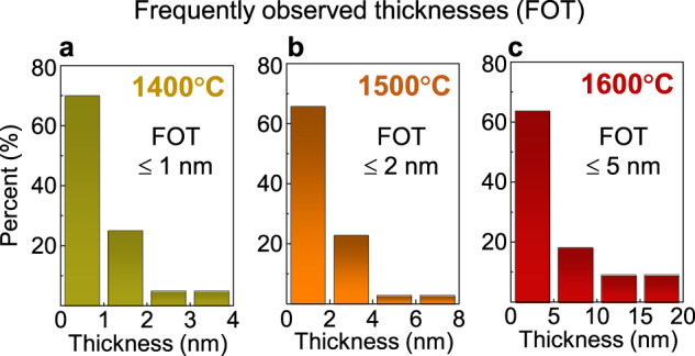
Since two major criteria for melting were proposed by Lindemann and Born in the early 1900s, many simulations and observations have been carried out to elucidate the premelting phenomena largely at the crystal surfaces and grain boundaries below the bulk melting point. Although dislocations and clusters of vacancies and interstitials were predicted as possible origins to trigger the melting, experimental direct observations demonstrating the correlation of premelting with lattice defects inside a crystal remain elusive. Using atomic-column-resolved imaging with scanning transmission electron microscopy in polycrystalline BaCeO3, here we clarify the initiation of melting at two-dimensional faults inside the crystals below the melting temperature. In particular, melting in a layer-by-layer manner rather than random nucleation at the early stage was identified as a notable finding. Emphasizing the value of direct atomistic observation, our study suggests that lattice defects inside crystals should not be overlooked as preferential nucleation sites for phase transformation including melting.


Conflict of interest statement

The authors declare no competing interests.

Figures

Fig. 1
Fig. 1. Structure and composition at RP faults in BaCeO3.
a–d A pair of HAADF and BF STEM images a, b is provided along with the enlargements c, d, indicating the image contrast for the presence of faults, as denoted by yellow arrows. The overall crystal structure of BaCeO3 is shown in the right-hand column. e The crystal structure of BaCeO3 is presented. f, g These two lower-magnification images demonstrate the various distribution of faults in a grain. h The image contrast of the fault is not clearly distinguished in the margined image. i However, the atomic-column-resolved EELS mapping directly demonstrates the two consecutive Ba−Ba columns at the fault plane. j An atomic array illustration along with the map is also provided for verification.
Fig. 2
Fig. 2. Bond characteristics at RP faults in BaCeO3.
a The crystal structure of BaCeO3 is presented. b This DOS plot indicates a strong overlap between the O 2p and Ce 4d states in contrast to no overlap of the Ba 5p states with the electronic states of oxygen below the Fermi level. Consequently, a high degree of covalency in Ce−O bonding is represented. c In good agreement with the DOS plot, A high electronic density between Ce and O is visualized in this isosurface contour map, as specifically illustrated in the Ce−O contour in the upper right panel. In contrast, no substantial electron density is noted between Ba and O at the fault plane in the lower right panel.
Fig. 3
Fig. 3. Observation of premelting at the faults.
a The loss of column contrast by melting is easily observable in both HAADF and BF imaging modes. As denoted by a pair of white lines in each HAADF image, the amorphous layer becomes thicker with increasing the post-annealing temperature. b A schematic illustration depicts the observation of the fractured surface by SEM. c Before premelting at the faults in the pellet sintered at 1330 °C, the overall microstructure of the fractured surface exhibits typical polycrystalline microstructure consisting of grains and grain boundaries. d−f In contrast, micron-level cracks (white arrows) are frequently observed in all the samples post-annealed at 1400 °C (d), 1500 °C (e), and 1600 °C (f), showing the either geometrically perpendicular or parallel configuration.
Fig. 4
Fig. 4. Three sets of HAADF images for the premelted fault regions at different temperatures.
a−c More than 10 grains in the [100] projection were observed in each case of post-annealing at 1400 (a), 1500 (b), and 1600 °C (c). It is noted that the thickness of the premelted amorphous layers is not completely constant at each annealing temperature but somewhat varies from fault to fault.
Fig. 5
Fig. 5. Thickness distributions of premelted amorphous layers.
a−c These bar graphs present the thickness distribution of amorphous layers in samples post-annealed at 1400 (a), 1500 (b), and 1600 °C (c). The amorphous layers become thicker, as the annealing temperature increases from 1400 to 1600 °C. Frequently observed thicknesses of amorphous layers in each graph are represented as the thicknesses observed at more than 60% of grain boundaries.
Fig. 6
Fig. 6. Layerwise premelting at the fault.
a An atomic illustration is provided in the first STEM image to verify the presence of a fault. b−d Images I−III (1400 °C) directly show the layer-by-layer behavior at the initial stage of premelting. Open circles represent the layers contacting atomic columns with low intensity due to significant atomic displacement by melting. e In image IV (1500 °C), melting of multiple atomic layers (more than four layers) is identified along with diffuse interfaces between the bulk crystal and the melted layer.
Fig. 7
Fig. 7. STEM image simulations.
a−d This series of simulated images and corresponding supercells demonstrates how the intensity of atom columns fades and nearly disappears, when the average atom displacement is 0 (a), 1.0 (b), 1.5 (c), and 2 Å (d). In the final image d, no distinct atomic columns are imaged in the layer where atoms substantially displace from their initial positions. e−h This series of simulated images shows how the atomic-column contrast in STEM images varies when melting occurs in a layer-by-layer manner: A [BaO] single layer (e), consecutive [BaO]−[BaO] layers (f), two [BaO]−[CeO2] layers (g), and four [BaO]–[CeO2] layers (h). In good agreement with the experimentally obtained STEM images shown in Fig. 6, these simulations consistently support layerwise premelting at the RP faults.
Fig. 8
Fig. 8. Recrystallization of a premelted amorphous layer.
a−c These HAADF images were captured from the video clip (Supplementary Movie 1) recorded during e-beam irradiation at 60 (a), 80 (b), and 120 s (c) in STEM. The regeneration of a periodic array of atomic columns is visualized, directly indicating the recrystallization. d An atomic array illustration is also provided to indicate the presence of a fault.

References

    1. Frenken JWM, van der Veen JF. Observation of surface melting. Phys. Rev. Lett. 1985;54:134–137. doi: 10.1103/PhysRevLett.54.134. - DOI - PubMed
    1. Lipowsky R, Breuer U, Prince KC, Bonzel HP. Multicomponent order parameter for surface melting. Phys. Rev. Lett. 1989;62:913–916. doi: 10.1103/PhysRevLett.62.913. - DOI - PubMed
    1. Li B, et al. Modes of surface premelting in colloidal crystals composed of attractive particles. Nature. 2016;531:485–488. doi: 10.1038/nature16987. - DOI - PubMed
    1. Li Y, et al. In situ study on atomic mechanism of melting and freezing of single bismuth nanoparticles. Nat. Commun. 2017;8:14462. doi: 10.1038/ncomms14462. - DOI - PMC - PubMed
    1. Foster DM, Pavloudis T, Kioseoglou J, Palmer RE. Atomic-resolution imaging of surface and core melting in individual size-selected Au nanoclusters on carbon. Nat. Commun. 2019;10:2583. doi: 10.1038/s41467-019-10713-z. - DOI - PMC - PubMed