. 2023 Apr 21;14(1):2283.
doi: 10.1038/s41467-023-38024-4.

Structural-disorder-driven critical quantum fluctuation and localization in two-dimensional semiconductors

Affiliations

Structural-disorder-driven critical quantum fluctuation and localization in two-dimensional semiconductors

Bong Gyu Shin et al. Nat Commun. .

Abstract

Quantum fluctuations of wavefunctions in disorder-driven quantum phase transitions (QPT) exhibit criticality, as evidenced by their multifractality and power law behavior. However, understanding the metal-insulator transition (MIT) as a continuous QPT in a disordered system has been challenging due to fundamental issues such as the lack of an apparent order parameter and its dynamical nature. Here, we elucidate the universal mechanism underlying the structural-disorder-driven MIT in 2D semiconductors through autocorrelation and multifractality of quantum fluctuations. The structural disorder causes curvature-induced band gap fluctuations, leading to charge localization and formation of band tails near band edges. As doping level increases, the localization-delocalization transition occurs when states above a critical energy become uniform due to unusual band bending by localized charge. Furthermore, curvature induces local variations in spin-orbit interactions, resulting in non-uniform ferromagnetic domains. Our findings demonstrate that the structural disorder in 2D materials is essential to understanding the intricate phenomena associated with localization-delocalization transition, charge percolation, and spin glass with both topological and magnetic disorders.


Conflict of interest statement

The authors declare no competing interests.

Figures
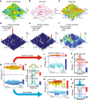
Fig. 1
Fig. 1. Curvature-induced charge localization and band edge flattening in monolayer MoS2.
a A 3D topographic STM image. b Local curvatures and c curvature-induced band gap fluctuation in the area of (a). df STS maps for localized and extended states for the intrinsic state of disordered MoS2. Localized peaks near (d) valence and (e) conduction band edges. f Extended states covered the whole measured surface. gi Curvature-induced band edge fluctuation at a neutral state. g VBM and CBM in the area of (a). h Structural model of a single cylindrical curvature, and (i) its CBM, VBM, and band gap (EG). jl Spatial flattening of CBM via electron-doping. j Band edges at electron-doped state (Δne = 5.67 × 1012 cm−2 (gate bias of 75 V)). Schematic plots of (k) doping charge localization and (l) its local band bending. mo Spatial flattening of VBM via hole-doping. m Band edges at hole-doped state (Δnh = 4.54 × 1012 cm−2 (gate bias of −60 V)). (Δne(h) denotes electron (hole) doping concentration). Schematic plots of (n) doping charge localization and (o) its local band bending. k, n Δρe(h) indicates electron (hole)-doping charge density. Purple lines indicate the Fermi level (EF). In all cases, the lengths of red and blue side bars indicate fluctuation ranges of CBM and VBM, respectively. Dashed lines indicate before-doping.
Fig. 2
Fig. 2. DFT calculations showing a spatial flattening of band edges in various 2D semiconductors.
a The variation of the LDOS depending on the doping concentration of monolayer MoS2 in cylindrical curvature structure. Corresponding atomic structure is shown under each column. Blue regions in LDOS indicate band gap. The Fermi level is set to zero (white-dashed line). Colored arrows at the top indicate the doping levels of each column. b Fluctuation range of band edges (ΔE) as a function of doping concentration (Δne) extracted from the theoretical results in (a). cg Doping induced spatial flattening of band edges in (c) MoSe2, (d) WSe2, (e) WS2, (f) MoTe2, and (g) WTe2. Doping levels are indicated at the top of each column in the unit of 1013 cm−2. All color scales for LDOS are the same in (a). h Fluctuation ranges of band edges as a function of the doping concentration of various 2D semiconducting monolayers, normalized by the maximum fluctuation range of CBM. In each plot, arb. denotes arbitrary units.
Fig. 3
Fig. 3. Charge localization at a curved MoS2.
a STM topography and b TBH mapping at 70 V of gate bias as electron-doping. ce the correlations among the averaged line profiles of (c) the surface morphology, (d) absolute curvature, and (e) relative TBH difference (ΔTBH) of the area shown in (a). The average values for plots were obtained in the axis of 12 nm in (a, b). (Supplementary Fig. 7 for each curvature value) The sample bias of −3 V was applied. f Structural model of curved monolayer MoS2. g Calculated doping charge density (∆ne) of ±2e/unit-cell in (f), where e is the electron charge and the sign of +(−) is the addition of electrons (holes). h Calculated local work function variation (ΔΦ) in (f) depending on the doping concentration. Electron-/hole-doping of ±2e/unit-cell is ±15.8 × 1013 cm−2. High curvature regions are red-shaded.
Fig. 4
Fig. 4. Criticality of metal–insulator transition and band tails in structurally disordered monolayer MoS2.
ad STS maps of the electron-doped MoS2 (data from Fig. 1j) near (a) VBM, (b) CBM, (c) at the critical energy (EC), and (d) above the critical energy. e Autocorrelation of the STS results in the electron-doped MoS2 (data from Fig. 1j). The interval between the dotted lines indicates the fluctuation range of the local conduction band edges. The critical energy (EC) is indicated by the arrow. The dashed line is ~ (ECE)ν, following the contour of the autocorrelation. The Fermi level is set to zero. f, Line profiles of the autocorrelation at different energies. The colored lines are fitted lines using the power law or exponential function. g Multifractal spectra and h, histograms of normalized LDOS at different energies. i Exponential band tails near the band edges, calculated by the tight-binding method. Inset shows scaled structural models corresponding to the strength of the disorder. Arrows indicate the protrusion of the band tails. j Correlation between the standard deviation of band gap distribution (σg) and band tail width (φc). The dash-dotted and dashed lines were fitting results by σg2 and σgp (p is a fitting parameter), respectively. The error bars indicate the standard deviations of data. The theoretical results were collected from the various surface morphologies with different roughness scaling. The experimental results of MoS2 on HOPG (height fluctuation ~±0.1 nm) and SiO2 (~±1 nm) are plotted. Each data point in (j) was obtained out of the several data sets. And each of the data sets includes over ~104 spectra. For each plot, arb. denotes arbitrary units.
Fig. 5
Fig. 5. Curvature-induced magnetism in monolayer MoS2.
a DFT-calculation of local magnetic moments in a spherical curvature structure of doped MoS2 (+4e/unit-cell). The surface of the structure is indicated by dots with the magnified z-axis for better visualization. Inset at the bottom is the atomic structure (4.74 × 4.38 nm2). b The calculated electron-doping charge density (Δρe) in the structure of (a). c A randomly deformed structural model of MoS2 (9.48 × 8.76 nm2) with the magnified z-axis. d DFT-calculated magnitude of local magnetization (ρ|m|) and e local magnetic moments in (c) with electron-doping (+66e/unit-cell), exhibiting localized non-uniform magnetic domains. The dots in (e) indicate the surface of (c) with the magnified z-axis.

References

    1. Evers F, Mirlin AD. Anderson transitions. Rev. Mod. Phys. 2008;80:1355. doi: 10.1103/RevModPhys.80.1355. - DOI
    1. Repin EV, Burmistrov IS. Mesoscopic fluctuations of the single-particle Green’s function at Anderson transitions with Coulomb interaction. Phys. Rev. B. 2016;94:245442. doi: 10.1103/PhysRevB.94.245442. - DOI
    1. Burmistrov IS, Gornyi IV, Mirlin AD. Multifractality at Anderson transition with Coulomb interaction. Phys. Rev. Lett. 2013;111:066601. doi: 10.1103/PhysRevLett.111.066601. - DOI - PubMed
    1. Cuevas E, Kravtsov VE. Two-eigenfunction correlation in a multifractal metal and insulator. Phys. Rev. B. 2007;76:235119. doi: 10.1103/PhysRevB.76.235119. - DOI
    1. Abrahams, E. (Ed.). 50 Years of Anderson Localization (World Scientific, 2010).