

Multiple Electronic Phases Coexisting under Inhomogeneous Strains in the Correlated Insulator
- PMID: 37097711
- PMCID: PMC10323623
- DOI: 10.1002/advs.202300789
Multiple Electronic Phases Coexisting under Inhomogeneous Strains in the Correlated Insulator
Abstract
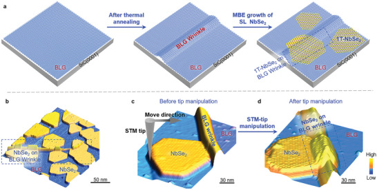
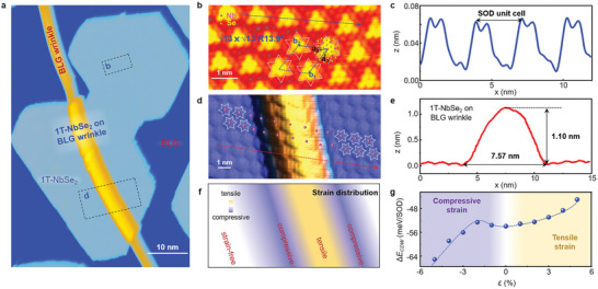
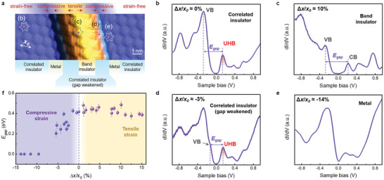
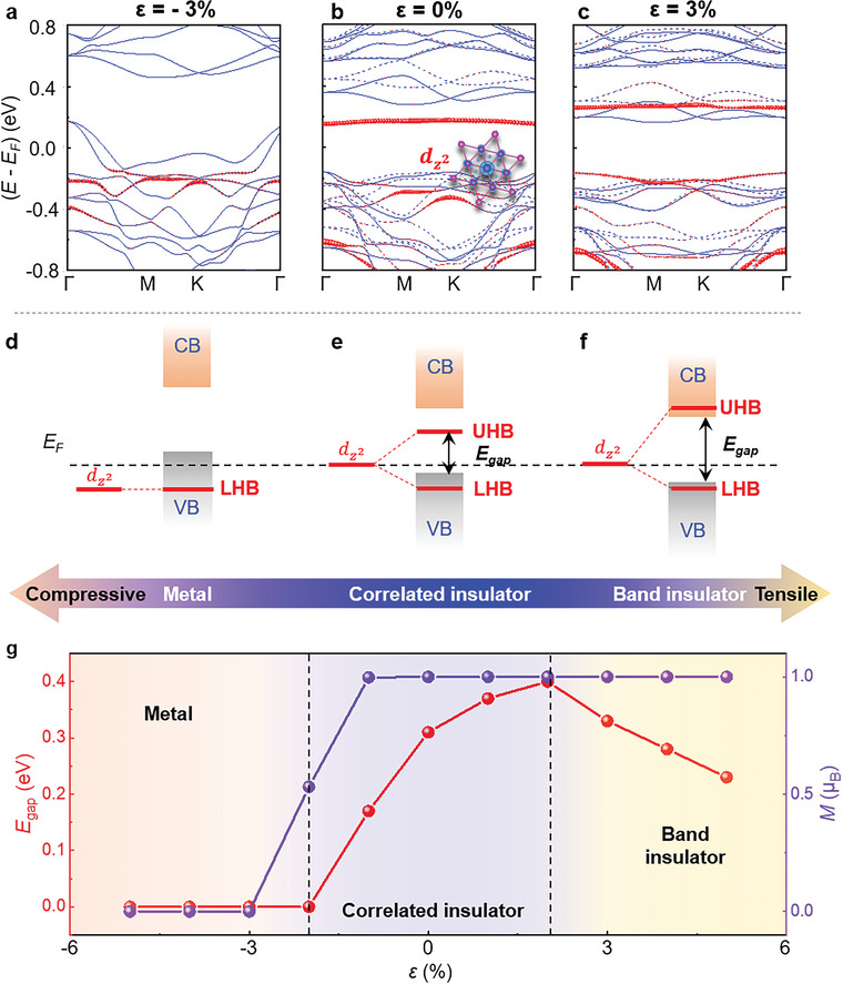
Monolayer transition metal dichalcogenides (TMDs) can host exotic phenomena such as correlated insulating and charge-density-wave (CDW) phases. Such properties are strongly dependent on the precise atomic arrangements. Strain, as an effective tuning parameter in atomic arrangements, has been widely used for tailoring material's structures and related properties, yet to date, a convincing demonstration of strain-induced dedicate phase transition at nanometer scale in monolayer TMDs has been lacking. Here, a strain engineering technique is developed to controllably introduce out-of-plane atomic deformations in monolayer CDW material 1T-NbSe2 . The scanning tunneling microscopy and spectroscopy (STM and STS) measurements, accompanied by first-principles calculations, demonstrate that the CDW phase of 1T-NbSe2 can survive under both tensile and compressive strains even up to 5%. Moreover, significant strain-induced phase transitions are observed, i.e., tensile (compressive) strains can drive 1T-NbSe2 from an intrinsic-correlated insulator into a band insulator (metal). Furthermore, experimental evidence of the multiple electronic phase coexistence at the nanoscale is provided. The results shed new lights on the strain engineering of correlated insulator and useful for design and development of strain-related nanodevices.
Keywords: charge-density-wave; correlated insulator; inhomogeneous strain; scanning tunneling microscopy.
© 2023 The Authors. Advanced Science published by Wiley-VCH GmbH.
Conflict of interest statement
The authors declare no conflict of interest.
Figures
Similar articles
-
Predicted multiple charge density wave phases in monolayer 1T-NbO2.J Phys Condens Matter. 2024 Feb 6;36(18). doi: 10.1088/1361-648X/ad22f9. J Phys Condens Matter. 2024. PMID: 38277682
-
Visualization of Confined Electrons at Grain Boundaries in a Monolayer Charge-Density-Wave Metal.Adv Sci (Weinh). 2024 Oct;11(37):e2306171. doi: 10.1002/advs.202306171. Epub 2023 Nov 20. Adv Sci (Weinh). 2024. PMID: 37984874 Free PMC article.
-
Robust charge-density wave strengthened by electron correlations in monolayer 1T-TaSe2 and 1T-NbSe2.Nat Commun. 2021 Oct 7;12(1):5873. doi: 10.1038/s41467-021-26105-1. Nat Commun. 2021. PMID: 34620875 Free PMC article.
-
Charge density waves in two-dimensional transition metal dichalcogenides.Rep Prog Phys. 2024 Apr 2;87(4). doi: 10.1088/1361-6633/ad36d3. Rep Prog Phys. 2024. PMID: 38518359 Review.
-
Surface/Interface Chemistry Engineering of Correlated-Electron Materials: From Conducting Solids, Phase Transitions to External-Field Response.Adv Sci (Weinh). 2021 Jan 5;8(4):2002807. doi: 10.1002/advs.202002807. eCollection 2021 Feb. Adv Sci (Weinh). 2021. PMID: 33643796 Free PMC article. Review.
Cited by
-
Realization of fractional-layer transition metal dichalcogenides.Nat Commun. 2025 Apr 17;16(1):3659. doi: 10.1038/s41467-025-59007-7. Nat Commun. 2025. PMID: 40246906 Free PMC article.
-
Atomic Manipulation of 2D Materials by Scanning Tunneling Microscopy: Advances in Graphene and Transition Metal Dichalcogenides.Nanomaterials (Basel). 2025 Jun 8;15(12):888. doi: 10.3390/nano15120888. Nanomaterials (Basel). 2025. PMID: 40559251 Free PMC article. Review.
References
-
- Dai Z., Liu L., Zhang Z., Adv. Mater. 2019, 31, 1805417. - PubMed
-
- Lee C., Wei X., Kysar J. W., Hone J., Science 2008, 321, 385. - PubMed
-
- Chen C., Wu J. Z., Lam K. T., Hong G., Gong M., Zhang B., Lu Y., Antaris A. L., Diao S., Guo J., Dai H., Adv. Mater. 2015, 27, 303. - PubMed
-
- Zhao B., Shen D., Zhang Z., Lu P., Hossain M., Li J., Li B., Duan X., Adv. Funct. Mater. 2021, 31, 2105.
-
- Miao Y., Zhao Y., Zhang S., Shi R., Zhang T., Adv. Mater. 2022, 34, 2200. - PubMed
Grants and funding
- 2022YFA1402602/National Key Research and Development Program of China
- 2020YFA0308800/National Key Research and Development Program of China
- 2021YFA1400100/National Key Research and Development Program of China
- 2022YFA1402502/National Key Research and Development Program of China
- 92163206/National Natural Science Foundation of China
LinkOut - more resources
Full Text Sources