. 2023 May 3;14(1):2530.
doi: 10.1038/s41467-023-38242-w.

Reconfigurable signal modulation in a ferroelectric tunnel field-effect transistor

Affiliations

Reconfigurable signal modulation in a ferroelectric tunnel field-effect transistor

Zhongyunshen Zhu et al. Nat Commun. .

Abstract

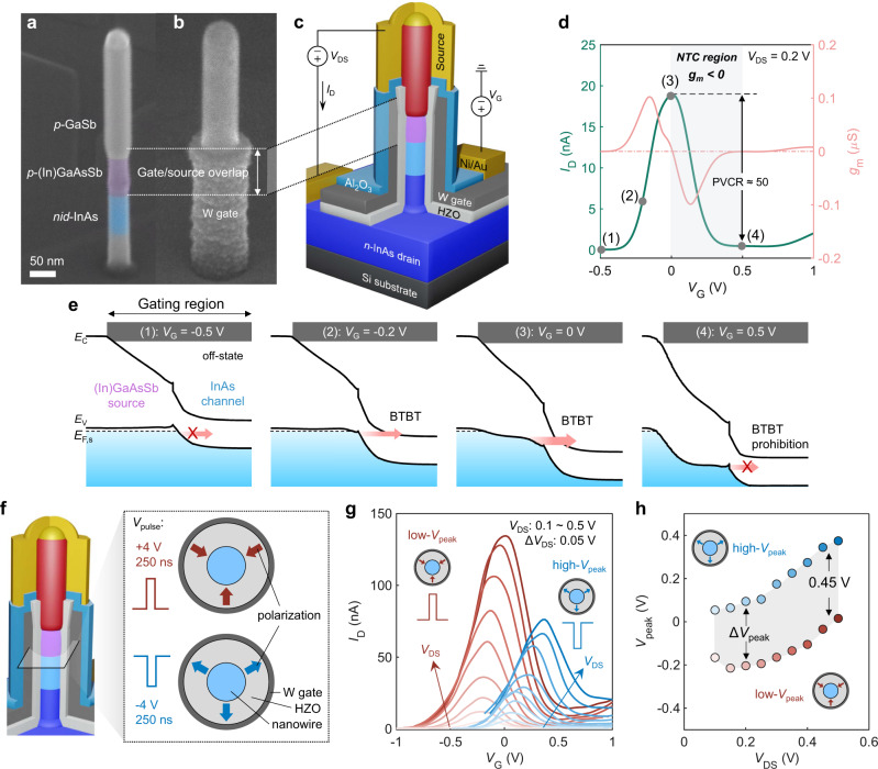
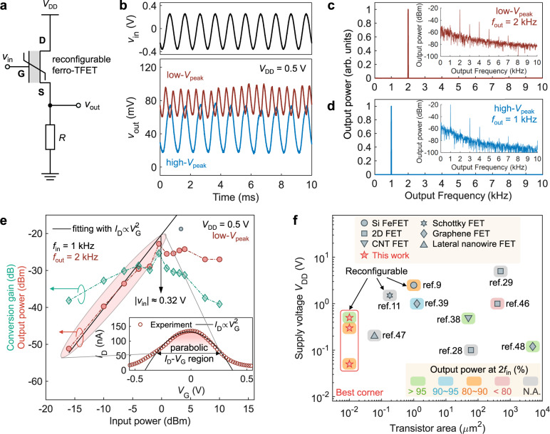
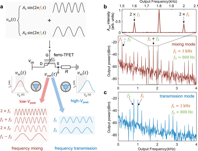
Reconfigurable transistors are an emerging device technology adding new functionalities while lowering the circuit architecture complexity. However, most investigations focus on digital applications. Here, we demonstrate a single vertical nanowire ferroelectric tunnel field-effect transistor (ferro-TFET) that can modulate an input signal with diverse modes including signal transmission, phase shift, frequency doubling, and mixing with significant suppression of undesired harmonics for reconfigurable analogue applications. We realize this by a heterostructure design in which a gate/source overlapped channel enables nearly perfect parabolic transfer characteristics with robust negative transconductance. By using a ferroelectric gate oxide, our ferro-TFET is non-volatilely reconfigurable, enabling various modes of signal modulation. The ferro-TFET shows merits of reconfigurability, reduced footprint, and low supply voltage for signal modulation. This work provides the possibility for monolithic integration of both steep-slope TFETs and reconfigurable ferro-TFETs towards high-density, energy-efficient, and multifunctional digital/analogue hybrid circuits.


Conflict of interest statement

The authors declare no competing interests.

Figures

Fig. 1
Fig. 1. Reconfigurable NTC in ferro-TFETs.
a, b SEM of (a) an as-grown nanowire heterostructure for a TFET and (b) a ferro-TFET post gate-length definition showing gate/source overlap. c Schematic of the final ferro-TFET device and the corresponding electrical measurement setup scheme. VG, applied gate voltage; VDS, source-drain bias; ID, drain current. d Transfer characteristic with NTC realized by geometrical gate/source overlap. e Schematic band diagrams at different VG defined in (d), demonstrating prohibited BTBT when further increasing VG. EC, the conduction band energy; EV, the valence band energy; EF,s, the Fermi level of the source. f Cross-sectional schematic of the nanowire channel region at which the polarization of the ferroelectric gate oxide can be used to reconfigure the TFET by applying a voltage pulse of +4 V or –4 V for 250 ns at the gate, respectively. g Transfer characteristics of a ferro-TFET with two different polarizations. Vpeak (defined as VG at the ID peak) in the I–V curves shows a positive shift when increasing VDS in both cases. Here, we define the two polarization states as low-Vpeak and high-Vpeak state, respectively, as displayed in the inset. h Vpeak as a function of VDS. ΔVpeak is defined as the difference between two peak voltages and increases with VDS.
Fig. 2
Fig. 2. Reconfigurable frequency doubling and phase shift in ferro-TFETs.
a The schematic of the electrical measurement setup with an alternating current (AC) signal as input for the ferro-TFET. The black scheme denotes the measured transfer characteristics while the red scheme indicates the gate voltage pulse (Vpulse) that sets the polarization in HZO gate oxide. Here, +Vpulse (+4 V/250 ns) and –Vpulse (–4 V/250 ns) represent binary ‘1’ and ‘0’, respectively. b The working principle for reconfigurable frequency doubling in the ferro-TFET. c Representative excerpt of the time-domain waveforms of vin (a sinusoidal wave with fin = 1 kHz) and iout. The same result is obtained after 10-cycle reconfigurations. This can be used for BFSK to encode data as ‘1’ and ‘0’ in communication systems. d The working principle for reconfigurable phase shift in the ferro-TFET. e The demonstration of the excerpt of the time-domain iout-vin for reconfigurable phase shift in ferro-TFETs.
Fig. 3
Fig. 3. Spectral analysis and low-power operation of reconfigurable ferro-TFETs.
a The schematic of measurement setup for output voltage (vout) waveform. D, G and S denote drain, gate, and source of the ferro-TFET, respectively. The resistor R = 8 MΩ. b Representative excerpt of the time-domain waveforms of vin and vout in two reconfigurable states. c, d The output power spectra of vout in the low-Vpeak (c) and high-Vpeak state (d), respectively. The inset shows the corresponding power spectrum in dBm. All the frequency spectra are obtained by applying the fast Fourier transform (FFT) algorithm with filtering the DC components. e The output power (at fout = 2 kHz) and the conversion gain of the ferro-TFET as a function of input power (at fin = 1 kHz) in the frequency doubling mode. The output power shows great overlay with the ideal parabolic IDVG fitting (black line) with respect to the input power up to ~0 dBm (amplitude of vin: |vin| ≈ 0.32 V). The inset shows the corresponding IDVG curve fitting with the ideal parabola (IDVG2). f Benchmarking of this work against other single-transistor frequency doublers. The transistor area from literature is based on the product of channel width and length or the estimation from the top-view microscope image. The operating frequency reported in listed work ranges from 10 Hz to 200 kHz. N.A. denotes “not available”.
Fig. 4
Fig. 4. Reconfigurable frequency mixing in a single ferro-TFET.
a Working principle of the reconfigurable frequency mixing controlled by the polarization in the ferroelectric gate oxide. b, c The power spectrum in (b) mixing mode and (c) transmission mode in the low-Vpeak state and high-Vpeak state, respectively. The magnified figure of (b) shows that the vout amplitude (Aout) intensity at f1 + f2 is almost twice that at 2f1 or 2f2, in agreement with the calculation result in Supplementary Note 1. Here, A1 = A2 = 0.3 V, f1 = 1 kHz, f2 = 800 Hz, VDD = 0.5 V, and R = 8 MΩ.

References

    1. Salahuddin S, Ni K, Datta S. The era of hyper-scaling in electronics. Nat. Electron. 2018;1:442–450. doi: 10.1038/s41928-018-0117-x. - DOI
    1. Rai, S. et al. Emerging reconfigurable nanotechnologies: can they support future electronics? In: 2018 IEEE/ACM International Conference on Computer-Aided Design (ICCAD) (IEEE, 2018).
    1. Heinzig A, Slesazeck S, Kreupl F, Mikolajick T, Weber WM. Reconfigurable silicon nanowire transistors. Nano Lett. 2012;12:119–124. doi: 10.1021/nl203094h. - DOI - PubMed
    1. Wu P, Reis D, Hu XS, Appenzeller J. Two-dimensional transistors with reconfigurable polarities for secure circuits. Nat. Electron. 2021;4:45–53. doi: 10.1038/s41928-020-00511-7. - DOI
    1. Breyer E. T., Mulaosmanovic H., Mikolajick T., Slesazeck S. Reconfigurable NAND/NOR logic gates in 28 nm HKMG and 22 nm FD-SOI FeFET technology. In: 2017 IEEE International Electron Devices Meeting (IEDM) 2851–2854 (IEEE, 2017).