Review
. 2023 May 5;13(20):13735-13785.
doi: 10.1039/d3ra01421e. eCollection 2023 May 2.

Organic and inorganic nanomaterials: fabrication, properties and applications

Affiliations
Review

Organic and inorganic nanomaterials: fabrication, properties and applications

Basmah H Alshammari et al. RSC Adv. .

Abstract

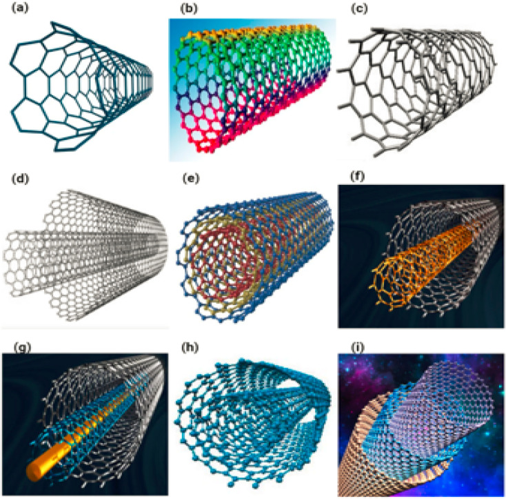
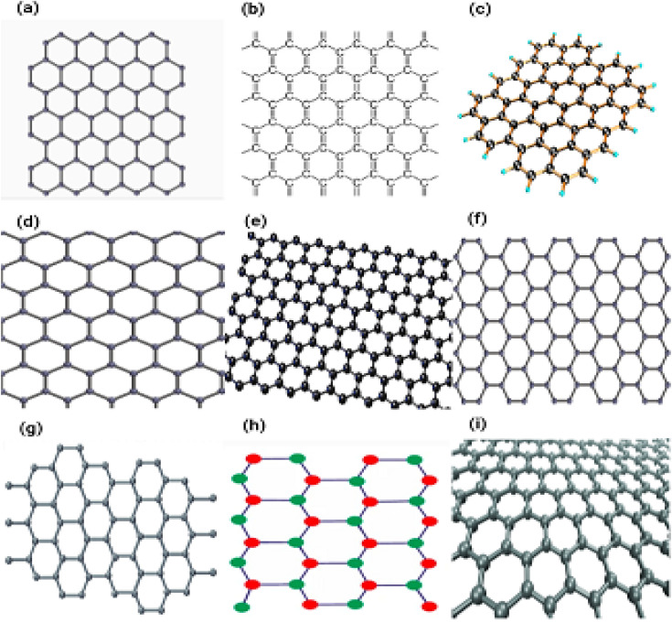
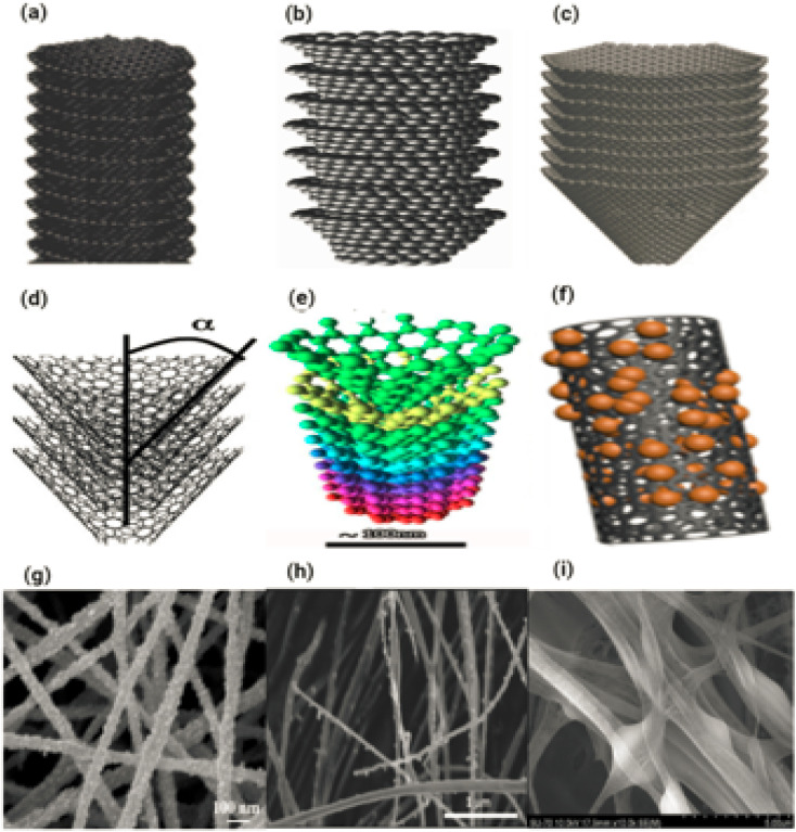
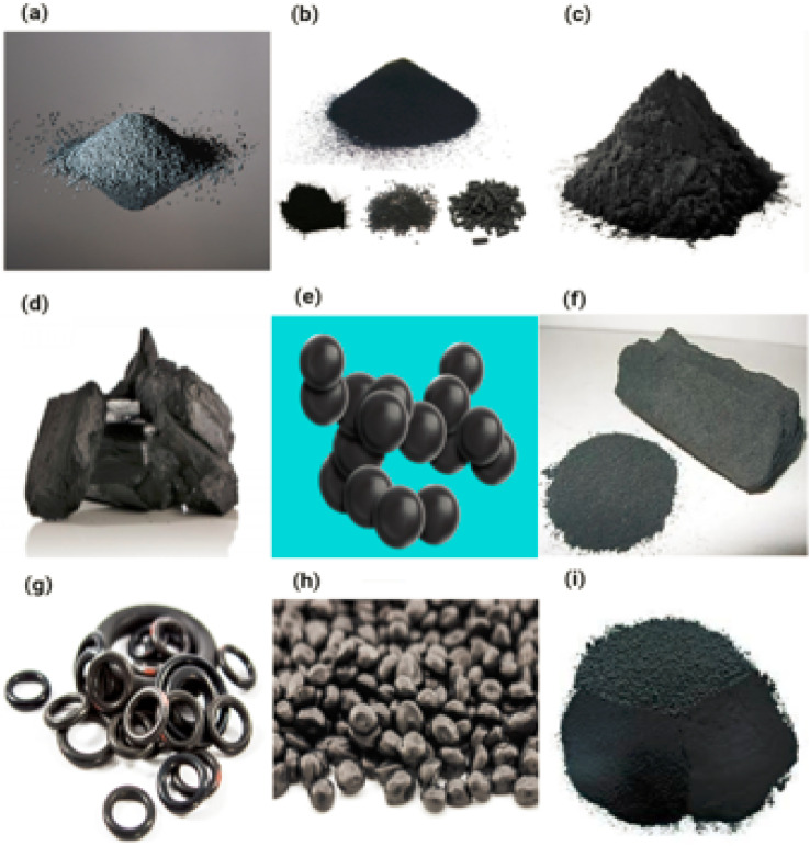
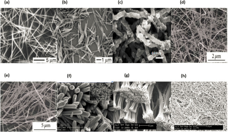
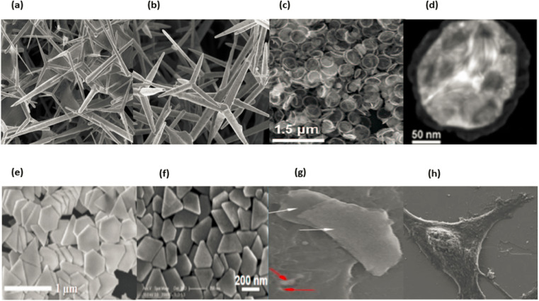
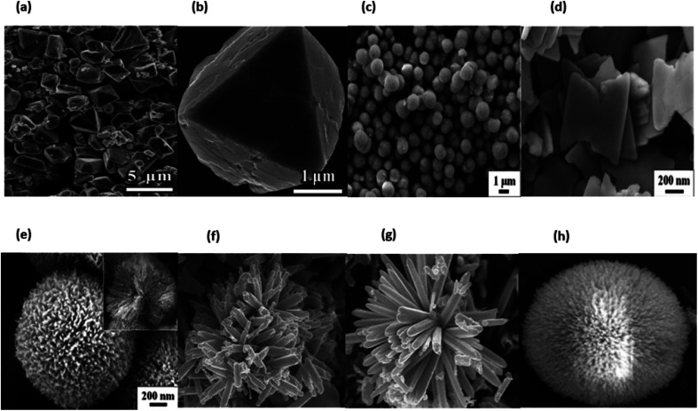
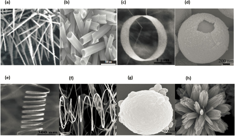
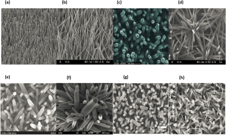
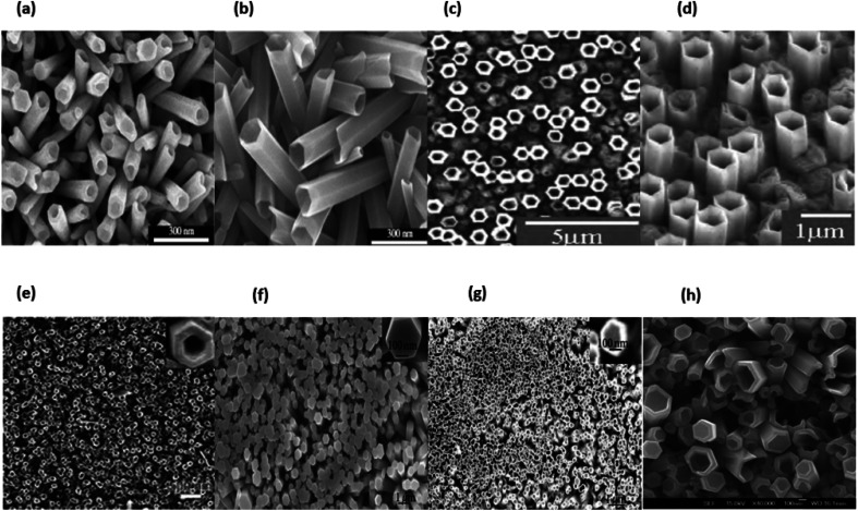
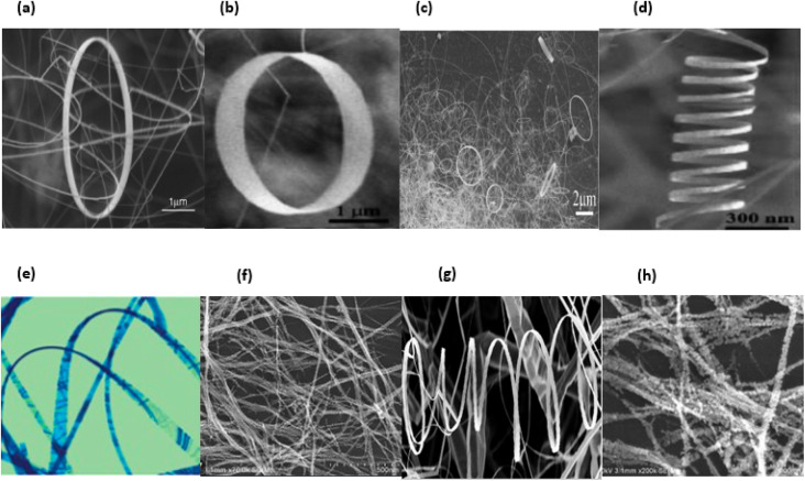
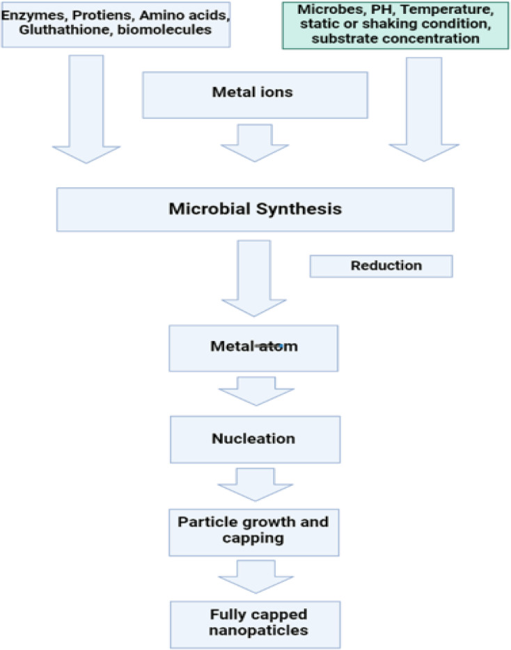
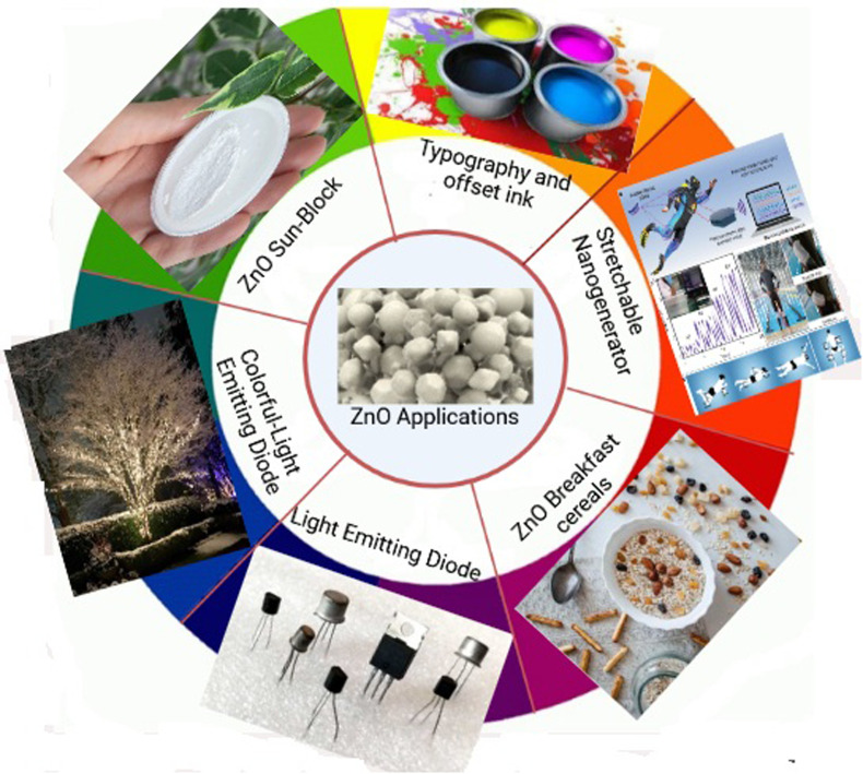
Nanomaterials and nanoparticles are a burgeoning field of research and a rapidly expanding technology sector in a wide variety of application domains. Nanomaterials have made exponential progress due to their numerous uses in a variety of fields, particularly the advancement of engineering technology. Nanoparticles are divided into various groups based on the size, shape, and structural morphology of their bodies. The 21st century's defining feature of nanoparticles is their application in the design and production of semiconductor devices made of metals, metal oxides, carbon allotropes, and chalcogenides. For the researchers, these materials then opened a new door to a variety of applications, including energy storage, catalysis, and biosensors, as well as devices for conversion and medicinal uses. For chemical and thermal applications, ZnO is one of the most stable n-type semiconducting materials available. It is utilised in a wide range of products, from luminous materials to batteries, supercapacitors, solar cells to biomedical photocatalysis sensors, and it may be found in a number of forms, including pellets, nanoparticles, bulk crystals, and thin films. The distinctive physiochemical characteristics of semiconducting metal oxides are particularly responsible for this. ZnO nanostructures differ depending on the synthesis conditions, growth method, growth process, and substrate type. A number of distinct growth strategies for ZnO nanostructures, including chemical, physical, and biological methods, have been recorded. These nanostructures may be synthesized very simply at very low temperatures. This review focuses on and summarizes recent achievements in fabricating semiconductor devices based on nanostructured materials as 2D materials as well as rapidly developing hybrid structures. Apart from this, challenges and promising prospects in this research field are also discussed.


Conflict of interest statement

The authors declared no potential conflicts of interest.

Figures

Fig. 1
Fig. 1. The Schematic diagram of organic nanoparticles.
Fig. 2
Fig. 2. Inorganic nanoparticles, metal and metal oxide nanoparticles are categorized as inorganic nanoparticles.
Fig. 3
Fig. 3. Metal nanomaterials.
Fig. 4
Fig. 4. Different types of metal and metal oxide-based nanomaterials.
Fig. 5
Fig. 5. SEM and TEM micrograph of SiO2 nanoparticles. (a) and (b) reproduced with permission. Copyright 2011, Nature, (c) reproduced with permission. Copyright 2012, Royal Society Chemistry. (d) Reproduced with permission. Copyright 2012, Royal Society of Open Science, (e) and (f) reproduced with permission. Copyright 201, Nature, (g) and (h) reproduced with permission. Copyright 2012, Royal Society Chemistry.
Fig. 6
Fig. 6. Bionanoparticles include exosomes, magnetosomes, lipoproteins, viruses and ferritin.
Fig. 7
Fig. 7. Carbon based nanomaterials. Carbon-based nanoparticles include carbon nanotubes, graphene, carbon nanofibers, fullerenes and carbon black.
Fig. 8
Fig. 8. (a–c) Shows the Fullerenes in different forms, C60 and (d–f) shows the C70 carbon nanotubes.
Fig. 9
Fig. 9. Single wall nanotubes are shown in (a–c), double wall nanotubes are shown in (d–f) and multiple wall nanotubes are shown in (g–i) which are made from graphene sheet.
Fig. 10
Fig. 10. (a–i) Displaying the different types of graphenes.
Fig. 11
Fig. 11. (a–i) Displaying the different type of carbon nanofibers.
Fig. 12
Fig. 12. (a–i) Displaying the carbon black.
Fig. 13
Fig. 13. Different types of 1D nanomaterials SEM images (a) and (b) nanorods & nanowires, reproduced with permission. Copyright 2003, WILEY-VCH, (c) nanofibers, (d) and (e) nanowires and nanoribbons, (f) nanosheets, (g) nanotubes and (h) nanowires.
Fig. 14
Fig. 14. Different types of 2D Nanomaterials SEM & TEM images, (a) and (b) ref. , (c)–(f) ref. , (g) and (h) ref. .
Fig. 15
Fig. 15. Different types of 3D Nanomaterials SEM & TEM images (a) and (b) ref. , (c)–(e) ref. , (f) and (g) ref. and (h) ref. .
Fig. 16
Fig. 16. Zinc oxide structure examples: (a) wires, (b) tubes, (c) rings, (d) cages, (e) springs, (f) belts, (g) spheres and (h) flowers.
Fig. 17
Fig. 17. Shows the different structures of ZnO (a) and (d) ref. , (b) and (e) ref. , (c) and (f) ref. .
Fig. 18
Fig. 18. Shows a model of ZnO with a hexagonal wurtzite structure. Zn–O tetrahedral coordination is demonstrated. The atoms of oxygen are depicted as larger white spheres, while the atoms of zinc are depicted as smaller brown spheres.
Fig. 19
Fig. 19. Typical ZnO doped optical properties graphs (a) ref. , (b) ref. , (c) ref. , (d) ref. , (e) ref. , (f) ref. .
Fig. 20
Fig. 20. Types of semiconductor (a) a magnetic semiconductor, (b) a dilute magnetic semiconductor and (c) a non-magnetic semiconductor.
Fig. 21
Fig. 21. Typical ZnO doped magnetic properties graphs (a) ref. , (b) ref. , (c) ref. , (d) ref. , (e) ref. , (f) ref. .
Fig. 22
Fig. 22. ZnO nanowires and rods SEM images (a) and (b) ref. , (c) ref. , (d) ref. , (f) ref. , (g) ref. , (h) ref. , (e) ref. .
Fig. 23
Fig. 23. Typical SEM images of ZnO nanotubes (a) and (b) ref. (c) and (d) ref. (e) ref. (f) and (g) ref. (h) ref. .
Fig. 24
Fig. 24. Typical SEM images of ZnO nanorings are shown in (a) ref. , (b) ref. , (c) ref. , (d) ref. and ZnO nanobelts are shown in (e) ref. , (f) ref. , (g) ref. , (h) ref. .
Fig. 25
Fig. 25. Typical SEM images of ZnO nanospheres and microspheres are shown in (a) and (b) ref. , (c) and (d) ref. , (e)–(g) ref. and (h) ref. .
Fig. 26
Fig. 26. Typical SEM images of ZnO nanostars and nanoflowers (a) and (b) ref. , (c) and (d) ref. , (e) and (f) ref. , (g) and (h) ref. .
Fig. 27
Fig. 27. Flow chart of co-precipitation method.
Fig. 28
Fig. 28. Flow chart sol–gel method.
Fig. 29
Fig. 29. Flow chart ZnO microemulsion method.
Fig. 30
Fig. 30. Flow chart ZnO hydrothermal method.
Fig. 31
Fig. 31. Flow chart ZnO hydrothermal method.
Fig. 32
Fig. 32. Flow chart SnO pyrolysis method.
Fig. 33
Fig. 33. Flow chart gas condensation method.
Fig. 34
Fig. 34. Flow chart high energy ball milling method.
Fig. 35
Fig. 35. Flow chart carbon nanotubes laser ablation method.
Fig. 36
Fig. 36. Flow chart ZnO plant mediated method.
Fig. 37
Fig. 37. Flow chart of microbes mediated method.
Fig. 38
Fig. 38. Schematic illustration of applications of the ZnO discussed below.
None
Muhammad Adil Mahmood
None
Aurangzeb Khan
None
Rajwali Khan

References

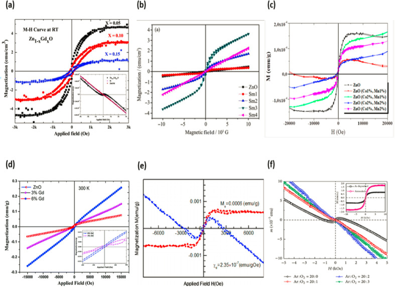
    1. Khan R. Shigidi I. Otaibi S. A. Althubeiti K. Abdullaev S. S. Rahman N. sohail M. Khan A. Iqbal S. Del Rosso T. Zaman Q. Khan A. Room temperature dilute magnetic semiconductor response in (Gd, Co) co-doped ZnO for efficient spintronics applications. RSC Adv. 2022;12:36126–36137. doi: 10.1039/D2RA06637H. - DOI - PMC - PubMed
    1. United Nations, Questions About Nanotechnology, 2012, https://www.epa.gov/chemical-research/research-nanomaterials, accessed Aug 21, 2014
    1. Considering Whether an FDA-Regulated Product Involves the Application of Nanotechnology, Federal Drug Administration, USA, 2011, https://www.fda.gov/RegulatoryInformation/Guidances/ucm257698.html, accessed Jan 25, 2016
    1. ISO/TS 80004-1:2010, Nanotechnology – Vocabulary – Part 1: Core Terms, International Organization for Standardization, Geneva, Switzerland, 2010, https://www.iso.org/standard/51240.html, accessed July 17, 2017
    1. Bleeker E. A. J., Cassee F. R., Geertsma R. E., de Jong W. H., Heugens E. H. W., Koers-Jacquemijns M., van De Meent D., Oomen A. G., Popma J., Rietveld A. G. and Wijnhoven S. W. P., Interpretation and implications of the European Commission's definition on nanomaterials; Letter report 601358001, RIVM, Bilthoven, Netherlands, 2012