. 2023 Apr 25;13(9):1460.
doi: 10.3390/nano13091460.

Broadband Optical Properties of Bi2Se3

Affiliations

Broadband Optical Properties of Bi2Se3

Georgy A Ermolaev et al. Nanomaterials (Basel). .

Abstract

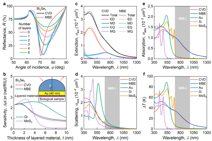
Materials with high optical constants are of paramount importance for efficient light manipulation in nanophotonics applications. Recent advances in materials science have revealed that van der Waals (vdW) materials have large optical responses owing to strong in-plane covalent bonding and weak out-of-plane vdW interactions. However, the optical constants of vdW materials depend on numerous factors, e.g., synthesis and transfer method. Here, we demonstrate that in a broad spectral range (290-3300 nm) the refractive index n and the extinction coefficient k of Bi2Se3 are almost independent of synthesis technology, with only a ~10% difference in n and k between synthesis approaches, unlike other vdW materials, such as MoS2, which has a ~60% difference between synthesis approaches. As a practical demonstration, we showed, using the examples of biosensors and therapeutic nanoparticles, that this slight difference in optical constants results in reproducible efficiency in Bi2Se3-based photonic devices.

Keywords: nanophotonics; optical constants; refractive index; spectroscopic ellipsometry; topological insulators; transition metal dichalcogenides.


Conflict of interest statement

The authors declare no conflict of interest.

Figures

Figure A1
Figure A1
Comparison of dielectric functions of chemical vapor deposition-grown [27] and exfoliated [12] MoS2.
Figure A2
Figure A2
Additional structural and morphological study of Bi2Se3. (a) Scanning electron microscopy image of Bi2Se3 surface. (b) X-ray diffraction pattern of Bi2Se3 with pronounced peaks which correspond to the (006), (009), (0012), (0015), (0018), and (0024) crystallographic planes of Bi2Se3.
Figure A3
Figure A3
Angular optical sensitivity of the SPR biosensor as a function of the thickness of the auxiliary Bi2Se3 layer. Calculations were performed neglecting the optical conductivity contribution from the topological surface states (red line) and accounting for this by adding a monolayer of graphene (gray line).
Figure 1
Figure 1
Bi2Se3 sample characterization. (a) Crystal structure of Bi2Se3. (b) Optical image of Bi2Se3 sample. (c) AFM color map of Bi2Se3 sample. (d,e) XPS spectra of Bi2Se3 with several Bi and Se peaks: Se3p1/2 (165.0 eV); Bi4f (BiOx) (164.2 eV); Bi4f5/2 (163.2 eV); Bi4f (BiOx) (158.9 eV); Bi4f7/2 (157.9 eV); Se3p3/2 (159.6 eV); Se-O (58.9 eV); Se0 (54.7 eV); Se3d3/2 (54.2 eV); Se3d5/2 (53.4 eV). Black, red, green, purple, blue, orange, violet, and cyan colors label experimental, total, Se3p1/2 or Se3p3/2, Bi4f (BiOx), Bi4f5/2 or Bi4f7/2, Se3d3/2, Se3d5/2, and Se0 XPS signals, respectively. Raman spectra of Bi2Se3 for (f) λ= 532 nm and (g) λ= 632.8 nm.
Figure 2
Figure 2
Variable-angle spectroscopic ellipsometry of Bi2Se3. Ellipsometry spectra of Bi2Se3 (a) Ψ and (b) Δ. Solid and dashed lines denote the experimental and calculated optical model data. (c) Refractive index and (d) extinction coefficient of Bi2Se3 for differently synthesized samples: chemical vapor deposition (CVD); density functional theory (DFT) calculations attributed to exfoliation; and molecular beam epitaxy (MBE), adopted from [40]. The inset in panel (c) is the calculated band structure of Bi2Se3. The inset in panel (d) shows a comparison between the experimental reflectance spectra of Bi2Se3 and the simulated one. Tabulated optical constants of Bi2Se3 are collected in Table A1.
Figure 3
Figure 3
Photonic applications of Bi2Se3. (a) The reflectance of the surface plasmon resonance (SPR) sensor based on a SiO2/Au (40 nm) chip with CVD and MBE-grown Bi2Se3. (b) The dependence of SPR sensor angular sensitivity on the thickness of Bi2Se3 layers. The inset is a schematic representation of an SPR sensor. For comparison, we also added the Gr and MoS2 performance. (c) The multipole decomposition of the extinction spectrum of a single Bi2Se3 nanosphere with a diameter d of 100 nm. (d) Extinction and (e) absorption cross-section of nanoparticles with diameters d of 100 nm for CVD and MBE-grown Bi2Se3. (f) Spectral dependence of the heating of nanoparticles with diameters d of 100 nm for CVD and MBE-grown Bi2Se3. The gray regions in panels c–f show spectral therapeutic region NIR-I (700–980 nm). For comparison, we included the performance of Au, Si, and MoS2 NPs.

References

    1. Khurgin J.B. Expanding the Photonic Palette: Exploring High Index Materials. ACS Photonics. 2022;9:743–751. doi: 10.1021/acsphotonics.1c01834. - DOI
    1. Baranov D.G., Zuev D.A., Lepeshov S.I., Kotov O.V., Krasnok A.E., Evlyukhin A.B., Chichkov B.N. All-Dielectric Nanophotonics: The Quest for Better Materials and Fabrication Techniques. Optica. 2017;4:814. doi: 10.1364/OPTICA.4.000814. - DOI
    1. Evlyukhin A.B., Novikov S.M., Zywietz U., Eriksen R.L., Reinhardt C., Bozhevolnyi S.I., Chichkov B.N. Demonstration of Magnetic Dipole Resonances of Dielectric Nanospheres in the Visible Region. Nano Lett. 2012;12:3749–3755. doi: 10.1021/nl301594s. - DOI - PubMed
    1. Ling H., Li R., Davoyan A.R. All van Der Waals Integrated Nanophotonics with Bulk Transition Metal Dichalcogenides. ACS Photonics. 2021;8:721–730. doi: 10.1021/acsphotonics.0c01964. - DOI
    1. Verre R., Baranov D.G., Munkhbat B., Cuadra J., Käll M., Shegai T. Transition Metal Dichalcogenide Nanodisks as High-Index Dielectric Mie Nanoresonators. Nat. Nanotechnol. 2019;14:679–684. doi: 10.1038/s41565-019-0442-x. - DOI - PubMed