. 2023 May 19;14(1):2873.
doi: 10.1038/s41467-023-38533-2.

Joule spectroscopy of hybrid superconductor-semiconductor nanodevices

Affiliations

Joule spectroscopy of hybrid superconductor-semiconductor nanodevices

A Ibabe et al. Nat Commun. .

Abstract

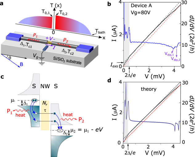
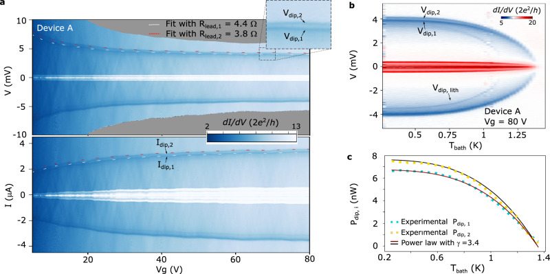
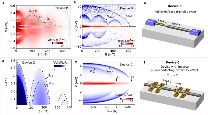
Hybrid superconductor-semiconductor devices offer highly tunable platforms, potentially suitable for quantum technology applications, that have been intensively studied in the past decade. Here we establish that measurements of the superconductor-to-normal transition originating from Joule heating provide a powerful spectroscopical tool to characterize such hybrid devices. Concretely, we apply this technique to junctions in full-shell Al-InAs nanowires in the Little-Parks regime and obtain detailed information of each lead independently and in a single measurement, including differences in the superconducting coherence lengths of the leads, inhomogeneous covering of the epitaxial shell, and the inverse superconducting proximity effect; all-in-all constituting a unique fingerprint of each device with applications in the interpretation of low-bias data, the optimization of device geometries, and the uncovering of disorder in these systems. Besides the practical uses, our work also underscores the importance of heating in hybrid devices, an effect that is often overlooked.


Conflict of interest statement

The authors declare no competing interests.

Figures

Fig. 1
Fig. 1. Principle of Joule spectroscopy.
a Schematics of the device geometry. A Josephson junction is formed by etching a 200-nm segment of a full-shell Al-InAs nanowire (NW). Voltage applied to a side gate, Vg, tunes the junction resistance, RJ. The balance between the Joule heat dissipated at the nanowire junction (equal to the product of the voltage, V, and current, I) and the cooling power from the superconducting leads 1 and 2 (P1 and P2) results in a temperature gradient along the device, T(x). At a critical value of Joule dissipation, the temperature of the leads, T0,1 and T0,2, exceed the superconducting critical temperature and the leads turn normal. Each lead can display different superconducting gaps Δ1 and Δ2. An external magnetic field, B, is applied with an angle θ to the NW axis. Tbath is the cryostat temperature. b I (solid black line) and differential conductance, dI/dV (solid blue line), as a function of V measured at Vg = 80 V in device A. For V < 2Δ/e, transport is dominated by Josephson and Andreev processes. By extrapolating the IV curve just above V = 2Δ/e, an excess current of Iexs ≈ 200 nA is estimated (dashed black line). Upon further increasing V, the Joule-mediated transition of the superconducting leads to the normal state manifests as two dI/dV dips (Vdip,1 and Vdip,2). These transitions fully suppress Iexs (dashed red line). c The nanowire is modeled as a quasi-ballistic conductor with N conduction channels with transmissions τ. We assume that the energy of the quasiparticles injected in the superconductors is fully converted into heat. d Keldysh-Floquet calculations of I(V) and dI/dV(V) using device A parameters (see Supplementary information for more information), reproducing the main features in (b).
Fig. 2
Fig. 2. Characterization of the superconductor-to-normal metal transition of the epitaxial Al leads.
a Gate voltage dependence of the dI/dV for device A. The data is plotted both as a function of V (top panel) and of I (bottom panel). Enhanced dI/dV features at low V and I can be attributed to Josephson and Andreev processes. Two dI/dV dips, which signal the superconductor-to-normal metal transition of the leads, can be identified in each of the panels (Vdip,i and Idip,i). The presence of the two dips is shown in greater detail in the inset of the top panel. The white and red dashed lines are fits to Eq. (3) with a single free fitting parameter per lead (Rlead,1 and Rlead,2). b dI/dV as a function of V and of Tbath. A faint dip at Vdip,lith is attributed to the Ti/Al contacts to the NW. c Pdip,1 = Vdip,1Idip,1/2 (blue squares) and Pdip,2 = Vdip,2Idip,2/2 (yellow squares) as a function of Tbath. The solid lines are fits to the power law in Eq. (4), yielding an exponent γ = 3.4.
Fig. 3
Fig. 3. Joule effect as a spectroscopical tool.
a Oscillations of Vdip,1 and Vdip,2 with applied magnetic field, which result from the modulation of Tc,i by the Little Parks (LP) effect. The dashed lines are fits to the Abrikosov–Gor'kov (AG) theory, from which we conclude that the primary cause for the different LP oscillations are differences in the superconducting coherence lengths of the leads. b Keldysh–Floquet calculations of the Andreev conductance at low V and of the dI/dV dips at high V as a function of B using device A parameters (Supplementary information to: Joule spectroscopy of hybrid superconductor-semiconductor nanodevices (2022).), capturing the main experimental observations. Panels (c) and (d) demonstrate the spectroscopical potential of the technique. c Zero-bias dV/dI normalized by the normal state resistance of the device. The dashed lines correspond to Tc,i(B) calculated with the AG parameters extracted by fitting the dips in panel (a). d Low-V transport characterization of device A as a function of B. The dashed lines show the spectral gaps, Ω1(B)/e (white) and Ω2(B)/e (green), and their sum, (Ω1(B) + Ω2(B))/e (black), obtained from Vdip,i(B).
Fig. 4
Fig. 4. Application of Joule spectroscopy to different NW devices.
a Low-bias transport characterization of device B as a function of magnetic field. Dashed lines show fittings of the spectral gaps, Ω1(B)/e (white) and Ω2(B)/e (green), and their sum, (Ω1(B) + Ω2(B))/e (black), obtained from Vdip,i(B). b Joule spectroscopy as a function of B clearly identifies that one of the superconducting leads is not doubly-connected, i.e., it behaves as a partial-shell lead. Dashed lines are fits to the AG theory. c Schematics of device B, as concluded from the Joule spectroscopy characterization (not to scale). d (dV/dI)/Rn as a function of T and B for device C. The dashed lines correspond to Tc,i obtained from Tc,i(B = 0) and the AG fits to Vdip,i(B) (not shown, see SI ). e T-dependence of Vdip,1 and Vdip,2 in device C. Lead 1 displays a lower critical temperature owing to its closer proximity to the lithographic Cr/Au contacts, as depicted in the schematics in panel f (not to scale).

References

    1. Sau JD, Lutchyn RM, Tewari S, Das Sarma S. Generic new platform for topological quantum computation using semiconductor heterostructures. Phys. Rev. Lett. 2010;104:040502. doi: 10.1103/PhysRevLett.104.040502. - DOI - PubMed
    1. Lutchyn RM, Sau JD, Das Sarma S. Majorana fermions and a topological phase transition in semiconductor-superconductor heterostructures. Phys. Rev. Lett. 2010;105:077001. doi: 10.1103/PhysRevLett.105.077001. - DOI - PubMed
    1. Oreg Y, Refael G, von Oppen F. Helical liquids and majorana bound states in quantum wires. Phys. Rev. Lett. 2010;105:177002. doi: 10.1103/PhysRevLett.105.177002. - DOI - PubMed
    1. Larsen TW, et al. Semiconductor-nanowire-based superconducting qubit. Phys. Rev. Lett. 2015;115:127001. doi: 10.1103/PhysRevLett.115.127001. - DOI - PubMed
    1. de Lange G, et al. Realization of microwave quantum circuits using hybrid superconducting-semiconducting nanowire josephson elements. Phys. Rev. Lett. 2015;115:127002. doi: 10.1103/PhysRevLett.115.127002. - DOI - PubMed