

Two-Dimensional Metal Halides for X-Ray Detection Applications
- PMID: 37209282
- PMCID: PMC10199999
- DOI: 10.1007/s40820-023-01118-1
Two-Dimensional Metal Halides for X-Ray Detection Applications
Abstract
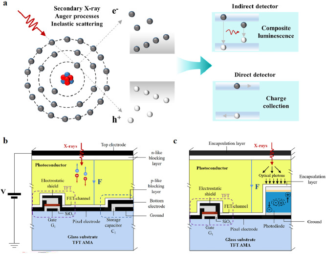
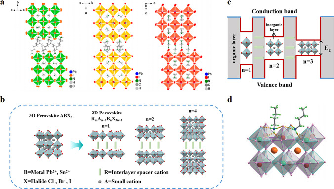
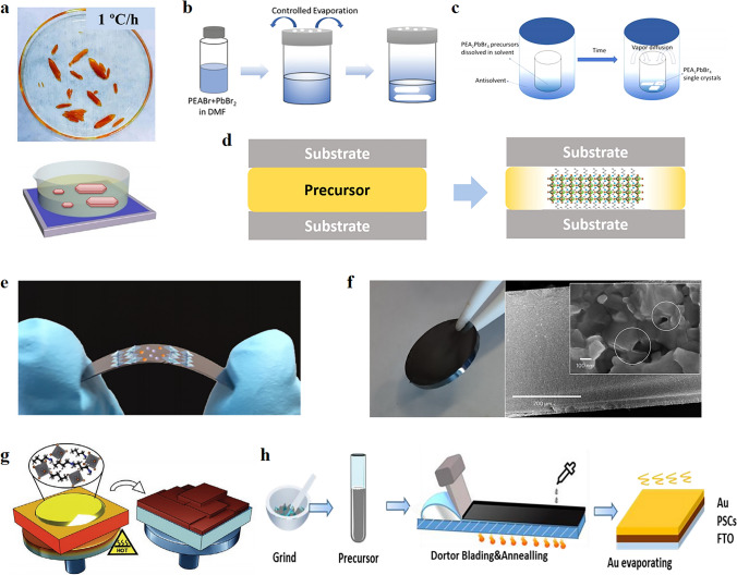
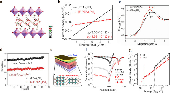
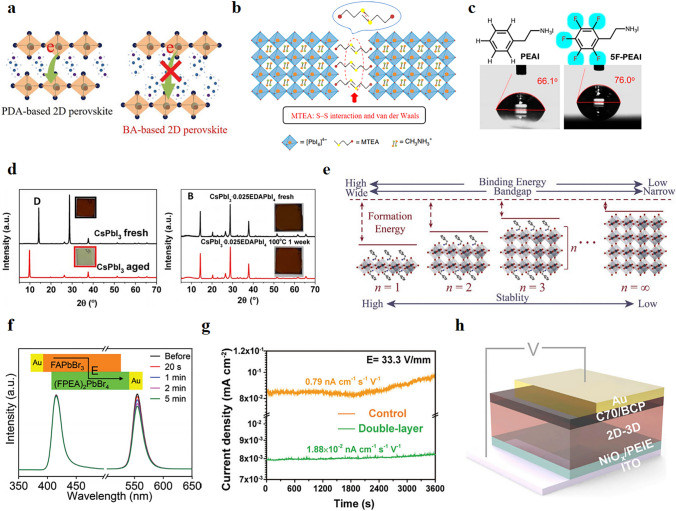
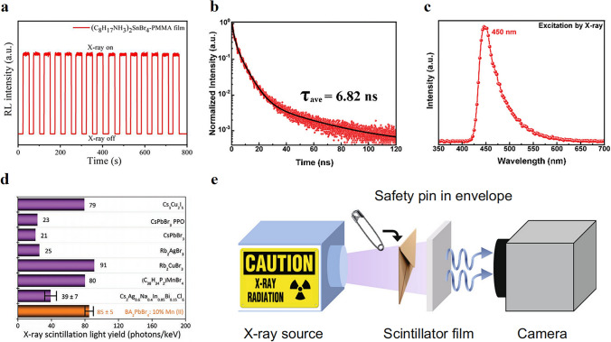
Metal halide perovskites have recently emerged as promising candidates for the next generation of X-ray detectors due to their excellent optoelectronic properties. Especially, two-dimensional (2D) perovskites afford many distinct properties, including remarkable structural diversity, high generation energy, and balanced large exciton binding energy. With the advantages of 2D materials and perovskites, it successfully reduces the decomposition and phase transition of perovskite and effectively suppresses ion migration. Meanwhile, the existence of a high hydrophobic spacer can block water molecules, thus making 2D perovskite obtain excellent stability. All of these advantages have attracted much attention in the field of X-ray detection. This review introduces the classification of 2D halide perovskites, summarizes the synthesis technology and performance characteristics of 2D perovskite X-ray direct detector, and briefly discusses the application of 2D perovskite in scintillators. Finally, this review also emphasizes the key challenges faced by 2D perovskite X-ray detectors in practical application and presents our views on its future development.
Keywords: Charge transport; High stability; Ion migration; Two-dimensional perovskite; X-ray Detector.
© 2023. The Author(s).
Conflict of interest statement
The authors declare no interest conflict. They have no known competing financial interests or personal relationships that could have appeared to influence the work reported in this paper.
Figures
Similar articles
-
Arising 2D Perovskites for Ionizing Radiation Detection.Adv Mater. 2024 Jun;36(26):e2309588. doi: 10.1002/adma.202309588. Epub 2024 Apr 23. Adv Mater. 2024. PMID: 38579272 Review.
-
High-Performance Flat-Panel Perovskite X-ray Detectors Enabled by Defect Passivation in Ruddlesden-Popper Perovskites.ACS Appl Mater Interfaces. 2024 Mar 20;16(11):14006-14014. doi: 10.1021/acsami.4c00232. Epub 2024 Mar 7. ACS Appl Mater Interfaces. 2024. PMID: 38450480
-
Progress and challenges in layered two-dimensional hybrid perovskites.Nanotechnology. 2022 Apr 29;33(29). doi: 10.1088/1361-6528/ac6529. Nanotechnology. 2022. PMID: 35390776
-
Recent advances in lead-free double perovskites for x-ray and photodetection.Nanotechnology. 2022 May 13;33(31). doi: 10.1088/1361-6528/ac6884. Nanotechnology. 2022. PMID: 35443239 Review.
-
3D/1D Perovskite Heterojunction for High-Performance Direct X-ray Detector.Small. 2025 May;21(21):e2501696. doi: 10.1002/smll.202501696. Epub 2025 Apr 15. Small. 2025. PMID: 40231552
Cited by
-
Research on the Technological Progress of CZT Array Detectors.Sensors (Basel). 2024 Jan 23;24(3):725. doi: 10.3390/s24030725. Sensors (Basel). 2024. PMID: 38339441 Free PMC article. Review.
-
Lattice Anchoring Stabilizes α-FAPbI3 Perovskite for High-Performance X-Ray Detectors.Nanomicro Lett. 2025 Jul 29;18(1):14. doi: 10.1007/s40820-025-01856-4. Nanomicro Lett. 2025. PMID: 40728710 Free PMC article.
-
Light Management in 2D Perovskite Toward High-Performance Optoelectronic Applications.Nanomicro Lett. 2025 Feb 6;17(1):131. doi: 10.1007/s40820-024-01643-7. Nanomicro Lett. 2025. PMID: 39909995 Free PMC article.
-
Stable self-powered X-ray detection with a low detection limit using a green halide hybrid perovskite ferroelectric crystal.Chem Sci. 2025 Feb 7;16(12):5283-5288. doi: 10.1039/d4sc06049k. eCollection 2025 Mar 19. Chem Sci. 2025. PMID: 40007662 Free PMC article.
-
Metal-Halide Perovskite Submicrometer-Thick Films for Ultra-Stable Self-Powered Direct X-Ray Detectors.Nanomicro Lett. 2024 Apr 26;16(1):182. doi: 10.1007/s40820-024-01393-6. Nanomicro Lett. 2024. PMID: 38668830 Free PMC article.
References
-
- Akcay S, Breckon T. Towards automatic threat detection: a survey of advances of deep learning within X-ray security imaging. Pattern Recogn. 2022;122:108245. doi: 10.1016/j.patcog.2021.108245. - DOI
-
- Szeles C. CdZnTe and CdTe materials for X-ray and gamma ray radiation detector applications. Phys. Status Solidi B. 2004;241(3):783–790. doi: 10.1002/pssb.200304296. - DOI
-
- Xu X, Qian W, Xiao S, Wang J, Zheng S, et al. Halide perovskites: a dark horse for direct X-ray imaging. EcoMat. 2020;2(4):e12064. doi: 10.1002/eom2.12064. - DOI
-
- G. Peng, B. An, H. Chen, Z. Li, Y. Xu et al., Self-organizing pixelated Cs4PbBr6 scintillator plate for large-area, ultra-flexible, high spatial resolution and stable X-ray imaging. Adv. Opt. Mater. 11(1), 2201751 (2022). 10.1002/adom.202201751
Publication types
LinkOut - more resources
Full Text Sources