Review
. 2023 May 24;15(1):134.
doi: 10.1007/s40820-023-01110-9.

Additive Engineering for Stable and Efficient Dion-Jacobson Phase Perovskite Solar Cells

Affiliations
Review

Additive Engineering for Stable and Efficient Dion-Jacobson Phase Perovskite Solar Cells

Min Liu et al. Nanomicro Lett. .

Abstract

Because of their better chemical stability and fascinating anisotropic characteristics, Dion-Jacobson (DJ)-layered halide perovskites, which owe crystallographic two-dimensional structures, have fascinated growing attention for solar devices. DJ-layered halide perovskites have special structural and photoelectronic features that allow the van der Waals gap to be eliminated or reduced. DJ-layered halide perovskites have improved photophysical characteristics, resulting in improved photovoltaic performance. Nevertheless, owing to the nature of the solution procedure and the fast crystal development of DJ perovskite thin layers, the precursor compositions and processing circumstances can cause a variety of defects to occur. The application of additives can impact DJ perovskite crystallization and film generation, trap passivation in the bulk and/or at the surface, interface structure, and energetic tuning. This study discusses recent developments in additive engineering for DJ multilayer halide perovskite film production. Several additive-assisted bulk and interface optimization methodologies are summarized. Lastly, an overview of research developments in additive engineering in the production of DJ-layered halide perovskite solar cells is offered.

Keywords: Additive compounds; Defect passivation; Dion–Jacobson phases; Perovskite solar cells; Stability.


Conflict of interest statement

The authors declare no conflict of interest.

Figures
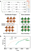
Fig. 1
Fig. 1
a DJ and RP phase structural comparison. The most often used DJ interlayer cations are: 1,3-propanediammonium (PDA), 1,4-butanediammonium (BDA), 3-(dimethylammonium)-1-propylammonium (DMAPA), 1,5-pentamethylenediammonium (PeDA), 1,6-hexamethylenediammonium (HDA), 1,8-octanediammonium (ODA), trans-1,4-cyclohexanediammonium (CHDA), 4-(aminomethyl)piperidinium (4-AMP), 3-(aminomethyl)piperidinium (3-AMP), p-phenylenediammonium (PPD), 1,4-phenylenedimethaneammonium (PDMA), 3-(aminomethyl)pyridinium (3-AMPY), 4-(aminomethyl)pyridinium (4-AMPY), m-phenylenediammonium (mPDA), 2,5-thiophenedimethylammonium (ThDMA) [50]. Copyright 2022, Wiley–VCH. b The best PCE evolution for RP and DJ PSCs for n ≤ 5 [51, 52]
Fig. 2
Fig. 2
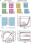
a Compare the Dion–Jacobson and Ruddlesden-Popper phases for perovskites made of oxide and halide. Crystal structure of CsBa2Ta3O10, Ca4Mn3O10 and (BA)2(MA)2Pb3I10 [83]; Copyright 2018, ACS. b An illustration of the crystal architecture in a schematic of the 2D-DJ perovskite (PDMA)(MA)n−1PbnI3n+1 (n = 4); c the hot-casting, antisolvent, and control devices' J-V curves and solar cell design, respectively; d For the three devices' champion cells, EQE and integrated short circuit current density (Jsc); e The steady-state power (SPO) and current density for the three devices were tested for 200 s at a permanent Voc close to the MPP [90]. Copyright 2021, Wiley–VCH
Fig. 3
Fig. 3
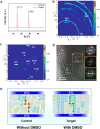
a The control and target layers' XRD patterns; b, c GIWAXS data for the reference and target movies; d Target film's HRTEM picture. FFT pictures of the relevant region are shown in the insets; e Diagrammatic representation of the control and target cells' morphologies and charge-transport schemes [101]. Copyright 2020, ACS
Fig. 4
Fig. 4
a PbI2's solubility in DMF both with and without 0.5 MACl; b XRD patterns of the layers made from raw PbI2 and PbI2 with 0.5 MACl; c Optical picture of the intermediate phase fiber made from (PXD)(MA)2Pb3I10 and its associated XRD pattern; d–e Graphics and visual images of the directed formation of PXD DJ PVK crystals at the liquid surface of the oversaturated precursor solution (n = 2) under the purposefully added (PXD)(MA)2Pb3I10 powder. f The right panel shows how the directed development of DJ perovskites is caused by the production of 3D-like perovskites on a PbI2-N,N-dimethylformamide (DMF)-based solvated phase (PDS) surface that has been soaked in DMF [115]. Copyright 2020, Wiley–VCH
Fig. 5
Fig. 5
a Diagram of the preparation procedure in a schematic of (BDA)FA4Pb5I16-xBrx; b Perovskite films' XRD patterns both with and without FABr post-treatment; c Spectra of UV–vis absorption and d the perovskite layers' band gap both before and after FABr treatment; e Diagram of the PSC's energy levels dependent on the control and desired PVK layers; f Dark I-V curves. [118] Copyright 2021, Elsevier
Fig. 6
Fig. 6
a Diagram depicting the progression of the (101) crystallographic plane's azimuth angle; b–e Polar intensity profiles along the ring at q = 0.95–1.08 Å − 1 assigned to the (101) plane of PVK layers with various SCN additives; f Diagram showing the development of the crystallographic plane (101)'s orientation as the quantity of NH4SCN added increases [125]. Copyright 2020, Wiley–VCH
Fig. 7
Fig. 7
a Curves of the control and target cell's current density and voltage; continuous testing of the goal and control devices [37]. Copyright 2022, ACS; b Curves illustrating the control and target device's current density vs voltage [131]. Copyright 2022, ACS
Fig. 8
Fig. 8
a Schematic representations of the crystallization of control and APSA-treated quasi-2D perovskite layers; b To assess the colloid size and dispersion in precursor solutions, use dynamic light scattering data. Inset: APSA's molecular construction. Characterizations of GIWAXS for (BA)2(MA)3Pb4I13, pristine, and APSA-treated (4-AMP)MAn−1PbnI3n+1 perovskite films, c–e an angle for grazing incidents of 0.1° and f–h at an angle of grazing incidence of 0.3°, respectively [100]. Copyright 2020, Nature Publishing Group
Fig. 9
Fig. 9
a The drawing of the PSC's inverted construction and cross-sectional SEM picture; b the control and target cell's current density–voltage curves in various scan directions; c the control and target cells' integrated Jsc curves and external quantum efficiency; d efficiency of control and target cells' steady-state outputs; e Stable testing of the control and target cells left unencapsulated in a glove box for more than 700 h; f PV parameter comparison between the control and target cells using statistics [150]. Copyright 2021, Wiley–VCH
Fig. 10
Fig. 10
a Cell structure, b a SEM cross-sectional picture, c J-V curve, d EQE spectrum, e stabilized PCE and Jsc, and f a histogram of PCEs collected from 50 FA-10-based DJ 2D PSC devices; g TRPL curves of films based on FA-0 and FA-10; h Jsc vs light intensity graphs that are double-logarithmic, and i VOC vs light intensity semilogarithmic graphs for the FA-0 and FA-10-based cells [161]. Copyright 2021, Wiley–VCH
Fig. 11
Fig. 11
a The single-solvent DMF-deposited DJ multilayer perovskite films' GIWAXS patterns, b DMF:DMSO, a binary solvent and c DMF:DMSO:NMP, a ternary solvent d TA spectra of the DJ PVK layers formed from the single-solvent DMF at various delay durations, e DMF:DMSO, a binary solvent and f ternary-solvent DMF:DMSO:NMP; g DJ PVK with random crystal orientation, even phase distribution, and graded phase distribution are shown schematically with h random and i vertical crystal orientation [163]. Copyright 2022, ACS
Fig. 12
Fig. 12
For the TiO2/perovskite surface's adsorption energy and charge redistribution, do the following DFT calculation: a PEA+'s electrostatic potential; b ordered C3N QD structure and c unorganized b-N-GQDs; d PEA+'s adsorption energy on TiO2 (101), e ordered C3N QDs and f disordered b-N-GQDs&TiO2 (101); views of the charge redistribution from above and from the side on g, h C3N QDs&TiO2 (101) and i, j b-N-GQDs&TiO2 (101) in the heterostructures [120]. Copyright 2022, Wiley–VCH
Fig. 13
Fig. 13
Illustration in schematic form of a Cs-doped DJ 2D perovskite [174]. Copyright 2022, Elsevier

Similar articles

Cited by

References

    1. Dahal B, Li W. Configuration of methylammonium lead iodide perovskite solar cell and its effect on the device's performance: a review. Adv. Mater. Interfaces. 2022;9(19):2200042. doi: 10.1002/admi.202200042. - DOI
    1. Dou Q, Whatley T, Syed T, Wei W, Wang H. Carbon nanomaterials-polymer composites for perovskite solar cells: preparation, properties and applications. J. Mater. Chem. A. 2022;10(37):19211–19230. doi: 10.1039/d2ta02175g. - DOI
    1. E.C. Kohlrausch, D.d.V. Freitas, C.I. da Silva Filho, L.F. Loguercio, L.A. Santa-Cruz et al., Advances in carbon materials applied to carbon-based perovskite solar cells. Energy Technol. 2200676 (2023). 10.1002/ente.202200676
    1. Luo X, Lin X, Gao F, Zhao Y, Li X, et al. Recent progress in perovskite solar cells: from device to commercialization. Sci. China-Chem. 2022;65(12):2369–2416. doi: 10.1007/s11426-022-1426-x. - DOI
    1. Sharma D, Mehra R, Raj B. Comparative study of hole transporting layers commonly used in high-efficiency perovskite solar cells. J. Mater. Sci. 2022;57(45):21172–21191. doi: 10.1007/s10853-022-07958-3. - DOI

LinkOut - more resources