Review
. 2023 May 24;10(1):24.
doi: 10.1186/s40580-023-00372-8.

Recent advancements of metalenses for functional imaging

Affiliations
Review

Recent advancements of metalenses for functional imaging

Dongmin Jeon et al. Nano Converg. .

Abstract

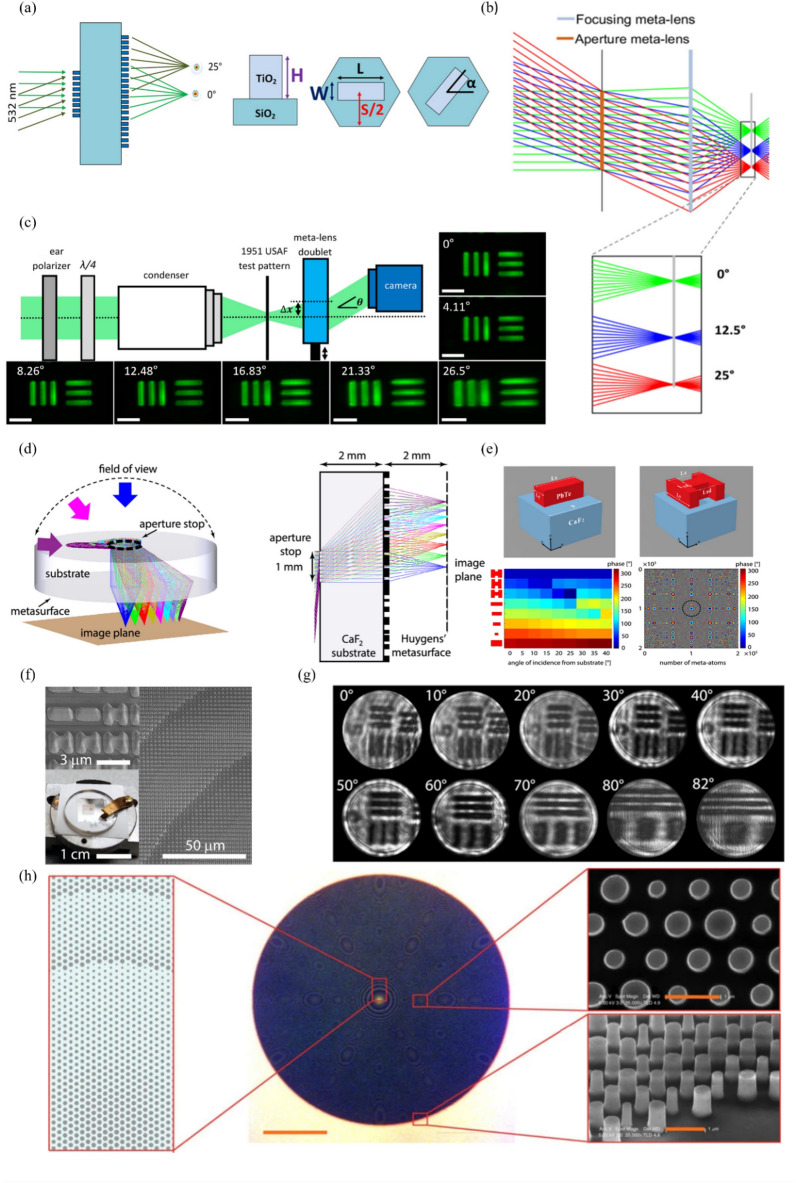
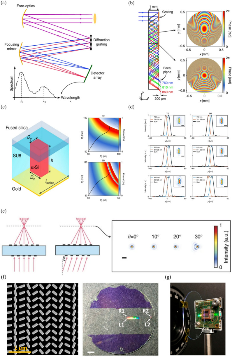
Metasurfaces can modulate light with periodically arranged subwavelength scatterers, and they can generate arbitrary wavefronts. Therefore, they can be used to realize various optical components. In particular, metasurfaces can be used to realize lenses, so-called metalenses. In the last decade, metalenses have been actively studied and developed. In this review, we firstly introduce the fundamental principles of metalenses in terms of materials, phase modulation method, and design method. Based on these principles, the functionalities and the applications can consequently be realized. Metalenses have a much larger number of degrees of freedom compared with that of existing refractive or diffractive lenses. Thus, they afford functionalities such as tunability, high numerical aperture, and aberration correction. Metalenses with these functionalities can be applied in various optical systems such as imaging systems and spectrometers. Finally, we discuss the future applications of metalenses.

Keywords: Aberration correction; Imaging system; Inverse design; Metalens; Metasurface; Numerical aperture; Phase modulation; Spectrometer; Tunability.


Conflict of interest statement

The authors declare that they have no competing interests.

Figures

Fig. 1
Fig. 1
Materials for metasurfaces and metalenses. a Schematic of plasmonic metalens and (inset) corresponding scanning electron microscopy (SEM) image (scale bar = 1 μm). Reproduced with permission [39] (Copyright 2012, Springer Nature). b Structure of MIM metasurface. MgF2 and gold films are located below the gold nanorod, leading to Fabry-Pérot-like behavior. Reproduced with permission [93] (Copyright 2015, Springer Nature). c SEM image of fabricated dielectric gradient metalens. d Measured intensity profile of metalens in xz-plane. c and d are reproduced with permission [94] (Copyright 2014, American Association for the Advancement of Science). e Comparison of visible transparency of (left) conventional and (right) low-loss a-Si:H. f Captured images of beam steering by low-loss a-Si:H metasurfaces. Deflected light with wavelengths of (top) 450 nm, (middle) 532 nm, and (bottom) 635 nm are shown. (e) and (f) are reproduced with permission [95] (Copyright 2021, Wiley-VCH).
Fig. 2
Fig. 2
Phase modulation methods. a Symmetric and antisymmetric mode of V-shaped gold antenna. b SEM image of plasmonic resonant-phase-based metasurface. (a) and (b) are reproduced with permission [103] (Copyright 2011, American Association for the Advancement of Science). c (top) Magnetic and (bottom) electric mode of Mie-resonant-phase-based metasurface. d Field amplitude and e phase spectrum of spectrally overlapped electric dipole and magnetic dipole resonances. c-e are reproduced with permission [97] (Copyright 2015, Wiley-VCH). f Side-view SEM image of propagation-phase-based metalens (scale bar = 600 nm). Reproduced with permission [41] (Copyright 2016, American Chemical Society). g (left) Two-fold and (right) three-fold symmetric meta-atoms in a square lattice. Reproduced with permission [104] (Copyright 2021, American Physical Society). h Simulated phase shift and second harmonic generation amplitude versus rotation angle of nonlinear meta-atom. i SEM image of fabricated nonlinear metalens. (h) and (i) are reproduced with permission [105] (Copyright 2022, American Association for the Advancement of Science). j Schematic of p2 space group unit. k Experimental intensity distributions (top) on the focal plane and (bottom) along the optical axis. (j) and (k) are reproduced with permission [106] (Copyright 2022, Springer Nature)
Fig. 3
Fig. 3
Inverse design of metalenses. a Comparison between (left) unit cell-based design and (right) inverse design. b Normalized intensity profile on longitudinal plane of inverse-designed high-NA achromatic metalens. Dotted lines indicate focal plane of metalens. (a) and (b) are reproduced with permission [110] (Copyright 2020, Optical Society of America). c Surrogate-model-based fast approximate solving of forward simulation. d Photograph of fabricated metalens with a diameter of 1 cm and achromatic and polarization-insensitive functionalities. (inset) SEM image of metalens (scale bar = 500 nm). e Experimental intensity distribution on xz-plane for wavelengths of (top) 488 nm, (middle) 532 nm, and (bottom) 658 nm. c-e are reproduced with permission [92] (Copyright 2022, Springer Nature). (f) Schematic of coupled-mode theory (CMT)-based forward simulation model. g Comparison of computation time between (red) single finite-element method simulations and (black) one iteration using CMT approach. f and g are reproduced with permission [111] (Copyright 2021, American Chemical Society)
Fig. 4
Fig. 4
Multifunctional and tunable metalenses. Multifunctional metalenses: a Measured normalized intensity distribution on xz-plane of varifocal metalens. θ represents polarization angle of incident light. Reproduced with permission [63] (Copyright 2019, American Chemical Society). b Schematic of nonlinear intensity multifunctional metalens. (inset) Transmission electron microscopy image of metallic quantum wells (scale bar = 5 nm). c Captured images for incident light intensity of (top) 5 GW/cm2 and (bottom) 20 GW/cm2 (scale bar = 200 μm). (b) and (c) are reproduced with permission [117] (Copyright 2022, Wiley-VCH). d Interleaving method for multiplexing multiple OAM modes in metalens. Reproduced with permission [118] (Copyright 2022, Springer Nature). Tunable metalenses: e Imaging experiment results of varifocal metalens for varying applied voltages. Voltages of 0 and 6 V produced clear images at distances of 692 and 732 μm, respectively (scale bar = 10 μm). Reproduced with permission [64] (Copyright 2018, American Chemical Society). f Experimental intensity profile of bifocal metalens on xz-plane for (top) LCP and (bottom) RCP incident light. Reproduced with permission [119] (Copyright 2021, Wiley-VCH). g Stretching condition of graphene-oxide-based metalens. This metalens is stretched uniformly, and the stretch ratio is 1.1 times. Reproduced with permission [120] (Copyright 2021, American Chemical Society). h Focal length change of GSST-based metalens. This metalens has different focal lengths in amorphous and crystalline states. i Measured focal spot profiles for (left) amorphous and (right) crystalline states. (inset) Captured images of focal spots. h and i are reproduced with permission [121] (Copyright 2021, Springer Nature)
Fig. 5
Fig. 5
High-NA metalenses. Optimization-based ultrahigh-NA metalenses: a Schematic of metalens designed using hybrid optimization algorithm. b Side-view SEM image of metalens. c Measured, simulated, and ideal intensity profiles of focal spot. Captured image of focal spot (inset). a-c are reproduced with permission [126] (Copyright 2018, American Chemical Society). d Structures of (left) conventional, (middle) topology-optimized, and (right) topology-optimized fabricable metalens (scale bar = 2 μm). e Simulated focusing efficiency of metalenses. Shaded area shows the region between the efficiency of conventional metalens and vector diffraction theory. (d) and (e) are reproduced with permission [116] (Copyright 2022, Wiley-VCH). Asymmetric-dimer-grating-based ultrahigh-NA metalenses: f Asymmetric dimer array and g side-view SEM image of metalens (scale bar = 500 nm). h Measured normalized intensity distribution on xz-plane. f-h are reproduced with permission [127] (Copyright 2018, American Chemical Society). i Adaptively arranged asymmetric dimers. Blue box shows Fresnel zones of metalens. j Focusing efficiency with different polarization angles. (insets) Point spread function for polarization angles of (left) 30°, (middle) 70°, and (right) 110°. k Three-dimensional image describing focusing performance of metalens. i-k are reproduced with permission [67] (Copyright 2022, Wiley-VCH)
Fig. 6
Fig. 6
Fiber- and waveguide-integrated metalenses. Fiber-integrated metalenses: a Schematic of a high-NA metafiber system. (inset) Measured focal plane in water (scale bar = 500 nm). b SEM image of integrated metalens (scale bar = 25 μm). (a) and (b) are reproduced with permission [76] (Copyright 2021, Springer Nature). c (top) Optical and (bottom) SEM images of achromatic metafiber. (d) SEM image of fabricated metalens on fiber end face. (e) Measured transverse FWHM and axial focal positions at different wavelengths. c-e are reproduced with permission [80] (Copyright 2022, Springer Nature). Waveguide-integrated metalenses: f Waveguide-integrated one-dimensional resonance-phase-based metalens. g Experimental intensity distribution of metalens. Field-emission SEM image of waveguide and metalens (inset). f and g are reproduced with permission [86] (Copyright 2020, American Association for the Advancement of Science). h Waveguide-integrated two-dimensional metalens. (inset) SEM image of metalens (scale bar = 500 nm). Reproduced with permission [88] (Copyright 2022, American Chemical Society). i Waveguide-integrated metalens based on geometric phase. j Simulated intensity distribution above one-dimensional metalens with (left) resonant phase and (right) geometric phase. i and j are reproduced with permission [87] (Copyright 2021, De Gruyter)
Fig. 7
Fig. 7
Monochromatic aberration compensation lens: a Schematic of metalens doublet. A metalens is present on both sides of the glass substrate. The meta-atoms of each lens have the same width, height, and length but have different angles. b Light incident from different angles forms images on the same image plane, with aberrations being compensated by an aperture metalens and a focusing metalens. c Schematic diagram of metalens doublet’s imaging setup and images for each angle of incidence (scale bar: 11 μm). a-c are reproduced with permission [129] (Copyright 2017, American Chemical Society). d Schematic diagram of an ultrawide-angle lens with an aperture and a metalens. e (top) Tilted view of a rectangular and an H-shaped meta-atom. (bottom left) Phase delay according to angle of incidence for each meta-atom shape. (bottom right) Metalens phase profile, where the black dashed circle indicates the aperture stop position and size. f SEM images of fabricated metalens. g Projected images of the 1951 USAF resolution test target with a period of 13.9 μm. d-g are reproduced with permission [130] (Copyright 2020, American Chemical Society). h Schematic and SEM images of polarization-insensitive metalens (scale bars: (center) 100 μm and (top- and bottom-right) 1 μm. Reproduced with permission [131] (Copyright 2015, Springer Nature)
Fig. 8
Fig. 8
Chromatic aberration compensation lens: a SEM image of fabricated achromatic metalens with NA = 0.106. (top left) Entire metalens (scale bar: 10 μm), and (top middle and right) magnified view of inset of 1st image (scale bar: 500 nm). (bottom) Experimental light intensity profile according to incident light at each wavelength. White dashed lines indicate the focal plane. Reproduced with permission [99] (Copyright 2018, Springer Nature). b (top left) Achromatic metalens using CP light. (top right) MgO meta-atom with height H, width W, and length L on a uniform periodic P × P substrate. (bottom left) Unit cell of simple metalens and hybrid metalens. θ is the angle that satisfies the phase according to the geometric PB phase method. (bottom right) top view of simple and hybrid metalenses with radius R. Reproduced with permission [134] (Copyright 2021, Springer Nature). c Schematic of an achromatic metalens that satisfies Eq. (4). The metalens is designed such that wavepackets from different locations can reach the focus simultaneously. Yellow line indicates a spherical wavefront. Reproduced with permission [135] (Copyright 2018, Springer Nature). d Schematic of a multilayer dielectric metalens operating at multiple wavelengths. Each layer provides a required hyperbolic phase profile for each different wavelength. Reproduced with permission [136] (Copyright 2018, American Chemical Society). e (left) Schematic of hybrid metalens that combines a phase plate and metalens to compensate for chromatic aberration while improving focusing efficiency. (right) Unit cell of hybrid metalens. Reproduced with permission [137] (Copyright 2020, Springer Nature). f Hybrid achromatic metalens (scale: cm). (left) Chromatic aberration correction and (right) spherical aberration correction. Reproduced with permission [138] (Copyright 2021, Optica Publishing Group). g Schematic of a dual-layer achromatic metalens (DAML). Planoconvex metalens, planoconcave metalens, and cross-section of DAML. Reproduced with permission [139] (Copyright 2020, Optica Publishing Group)
Fig. 9
Fig. 9
Imaging system using metalens: a Schematic of see-through near-eye display using metalens (ML), dichroic mirrors (DMs), beam splitter (BS), LCP, and RCP. b Schematic of operation principle of a metalens according to the incident direction of CP light and when combined with a circular polarizer. c Augmented reality (AR) images that combine a real object and virtual information and virtual reality (VR) images that only show virtual information with a fabricated achromatic metalens with NA = 0.106. a-c are reproduced with permission [128] (Copyright 2018, Springer Nature). d (left) Conventional CMOS image sensor (CIS) with microlenses and color filters and (right) CIS with full-color routing metalens. e SEM image of full-color routing metalens and a schematic of a multiplex unit cell. f Schematic of metalens causing the convergence of incident light at an arbitrary location F. O: center of metalens, B: arbitrary position on metalens surface, A: vertical projection point from focal point F onto metalens surface. d-f are reproduced with permission [100] (Copyright 2017, American Chemical Society). g (top) Schematic of conventional setup. WP : waveplate, PD : photodetector. (bottom) schematic of using metasurface. h Schematic diagram of a supercell with different polarization focus at different points. g and h are reproduced with permission [149] (Copyright 2018, American Chemical Society)
Fig. 10
Fig. 10
Spectrometer using metasurface: a Schematic of a conventional spectrometer. b Schematic of compact spectrometer using metasurface, and phase profile of metasurface compensating for monochromatic aberration. c (left) Structure of unit cell, and (top right and bottom) simulated phase according to TE and TM polarization, where the black curve represents Dx-Dy with the same phase for TE and TM polarization. d Intensity distribution when light with wavelength difference of 1.25 nm is incident with TE and TM polarization. a-d are reproduced with permission [156] (Copyright 2018, Springer Nature). e Schematic of a doublet metalens for on-axis and off-axis incidence, where the spot size is small owing to monochromatic aberration compensation (scale bar: 2 μm). Reproduced with permission [157] (Copyright 2016, Springer Nature). f (left) SEM image of fabricated metalens, and schematic of fabricated device with four separate metalenses. (right) R and L refer to the helicity of light focused by each metalens, and 1 and 2 indicate the parameters used for the lens design (scale bar: 5 mm). g Compact spectrometer that combines a metalens and a CMOS camera. f and g are reproduced with permission [158] (Copyright 2017, AIP Publishing)

References

    1. Yu YF, et al. High-transmission dielectric metasurface with 2π phase control at visible wavelengths. Laser Photonics Rev. 2015;9(4):412–418. doi: 10.1002/lpor.201500041. - DOI
    1. Wan W, Gao J, Yang X. Full-color plasmonic metasurface holograms. ACS Nano. 2016;10(12):10671–80. doi: 10.1021/acsnano.6b05453. - DOI - PubMed
    1. Kim M, et al. Reaching the highest efficiency of spin Hall effect of light in the near-infrared using all-dielectric metasurfaces. Nat. Commun. 2022;13(1):2036. doi: 10.1038/s41467-022-29771-x. - DOI - PMC - PubMed
    1. Zheng G, et al. Full-space metasurface holograms in the visible range. Opt. Express. 2021;29(2):2920–2930. doi: 10.1364/OE.417202. - DOI - PubMed
    1. Kim G, et al. Metasurface-driven full-space structured light for three-dimensional imaging. Nat. Commun. 2022;13(1):5920. doi: 10.1038/s41467-022-32117-2. - DOI - PMC - PubMed

LinkOut - more resources