Review
. 2023 May 17;14(5):1060.
doi: 10.3390/mi14051060.

Integrated Graphene Heterostructures in Optical Sensing

Affiliations
Review

Integrated Graphene Heterostructures in Optical Sensing

Phuong V Pham et al. Micromachines (Basel). .

Abstract

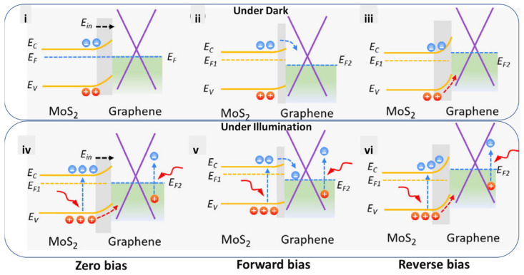
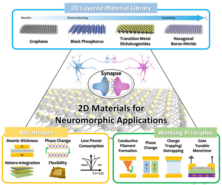
Graphene-an outstanding low-dimensional material-exhibited many physics behaviors that are unknown over the past two decades, e.g., exceptional matter-light interaction, large light absorption band, and high charge carrier mobility, which can be adjusted on arbitrary surfaces. The deposition approaches of graphene on silicon to form the heterostructure Schottky junctions was studied, unveiling new roadmaps to detect the light at wider-ranged absorption spectrums, e.g., far-infrared via excited photoemission. In addition, heterojunction-assisted optical sensing systems enable the active carriers' lifetime and, thereby, accelerate the separation speed and transport, and then they pave new strategies to tune high-performance optoelectronics. In this mini-review, an overview is considered concerning recent advancements in graphene heterostructure devices and their optical sensing ability in multiple applications (ultrafast optical sensing system, plasmonic system, optical waveguide system, optical spectrometer, or optical synaptic system) is discussed, in which the prominent studies for the improvement of performance and stability, based on the integrated graphene heterostructures, have been reported and are also addressed again. Moreover, the pros and cons of graphene heterostructures are revealed along with the syntheses and nanofabrication sequences in optoelectronics. Thereby, this gives a variety of promising solutions beyond the ones presently used. Eventually, the development roadmap of futuristic modern optoelectronic systems is predicted.

Keywords: integrated graphene heterostructure; optical sensing; optical waveguide; perspective; plasmonic; spectrometer; synaptic system.


Conflict of interest statement

The authors declare no conflict of interest.

Figures

Figure 1
Figure 1
Merits of the optical responsivity performances of optical sensing systems under the broad absorption band (UV to IR) using representative integrated 2D heterostructures. Adopted with permission from Ref. [18]. Copyright 2022 American Chemical Society.
Figure 2
Figure 2
The general mechanism of low-dimensional material-based optical sensing (a) Photoconductive effect, (b) Photogating effect, (c) Electromagnetic effect, (d) Photovoltaic effect, (e) Photothermoelectric effect, (f) Bolometric effect, and (g) Plasma-wave effect. (ag) are reproduced with permission from Ref. [2]. Copyright 2021 Wiley.
Figure 3
Figure 3
The optical sensing mechanism depicted for representative graphene-integrated heterostructures (MoS2/graphene/Si). (iiii) The band diagrams under zero bias, (i) forward bias, (ii) reverse bias, and (iii) in the dark. (ivvi) The band diagrams under zero bias, (iv) forward bias, (v) reverse bias, and (vi) under illumination. Reproduced with permission from Ref. [3]. Copyright 2021 Wiley.
Figure 4
Figure 4
The foremost representative applications of integrated graphene heterostructures in optoelectronics.
Figure 5
Figure 5
hBN/graphene/WSe2/hBN-based integrated heterostructures for ultrafast optical sensing. Reproduced with permission from Ref. [22]. Copyright 2021 Nature Publishing Group.
Figure 6
Figure 6
Graphene-based plasmonic systems. (a) Au NPs/rGO/Au thin films-integrated plasmonic optical systems. Reproduced with permission from Ref. [25]. Copyright 2021 Springer. Graphene-integrated hybrid structures for optical sensing. (b) Graphene–disk plasmonic resonators connected by quasi-1D graphene nanoribbons. (c) An Au nanogap antenna with graphene in the gap. The scale bar is 100 nm (5 μm for inset). (d) Finger type Ti/Au plasmonic nanostructures on graphene. The right figure indicates the photovoltage map, illuminated with 514 nm light with transverse polarization. The scale bar is 1 μm. (e) Graphene photodetector with AuNPs (left) and SEM image of AuNPs on a graphene surface (right). The scale bar is 100 nm. (f) A single Au heptamer sandwiched between two monolayer graphene sheets (left) and a SEM image of a Au heptamer (right). The scale bar in the inset of the right figure is 100 nm. (g) Au-patched graphene nano-stripes for utilizing maximum metal–graphene interfaces for enhanced photocurrent. (h) A graphene photodetector integrating both optical heating enhancement (via gap plasmonic structures) and electrical junction enhancement (via split gates). (i) A single photon detection device using a Josephson junction. (bi) Reproduced with permission from Ref. [24]. Copyright 2022 Springer.
Figure 7
Figure 7
An optical waveguide using graphene heterostructures for electronic photonic integrated circuits configured on a chip. Reproduced with permission from Ref. [39]. Copyright 2018 Elsevier.
Figure 8
Figure 8
Schematic (a) and OM image (b) of Si PPC/BN/graphene heterostructure-based photonic crystal nanocavity. (a,b) are reproduced with permission from Ref. [54]. Copyright 2015 American Chemical Society.
Figure 9
Figure 9
Computational optical spectrometers adopted for spectral-to-spatial mapping: (a) a disordered photonic chip [57], (b) a spiral waveguide [58], (c) a dispersive hole array [59], (d) a polychromator [60], (e) colloidal quantum dot mixtures [61], (f) photonic crystal slabs [62], (g) arrays of structurally colored nanowires [63], (h) a single compositionally engineered nanowire [64]. Reproduced with permission from Ref. [65]. Copyright 2021 AAAS.
Figure 10
Figure 10
Optoelectronic synaptic systems. An overview of neuromorphic applications, based on representative 2D materials and graphene/MoS2 nanostructure-based synaptic devices. Reproduced with permission from Ref. [90]. Copyright 2020 Elsevier.
Figure 11
Figure 11
A possible roadmap of 2D graphene integration heterostructure systems-based future optoelectronics: perspectives for the development and challenges from the material synthesis step to the integrated system step.
Figure 12
Figure 12
The promising research branches of new graphene/2D materials-integrated heterostructure stacks.
Figure 13
Figure 13
The prediction of the development roadmap of future modern optoelectronic systems.

References

    1. Rogalski A., Kopytko M., Martyniuk P. 2D Material Infrared and Terahertz Detectors: Status and Outlook. Opto-Electron. Rev. 2020;28:107–154.
    1. Qiu Q., Huang Z. Photodetectors of 2D Materials from Ultraviolet to Terahertz Waves. Adv. Mater. 2021;33:2008126. doi: 10.1002/adma.202008126. - DOI - PubMed
    1. Liu R., Wang F., Liu L., He X., Chen J., Li Y., Zhai T. Band Alignment Engineering in Two-Dimensional Transition Metal Dichalcogenide-Based Heterostructures for Photodetectors. Small Struct. 2021;2:2000136. doi: 10.1002/sstr.202000136. - DOI
    1. Yao J., Yang G. 2D Material Broadband Photodetectors. Nanoscale. 2020;12:454–476. doi: 10.1039/C9NR09070C. - DOI - PubMed
    1. Aamir Iqbal M., Malik M., Khac Le T., Anwar N., Bakhsh S., Shahid W., Shahid S., Irfan S., Al-Bahrani M., Morsy K., et al. Technological Evolution of Image Sensing Designed by Nanostructured Materials. ACS Mater. Lett. 2023;5:1027–1060. doi: 10.1021/acsmaterialslett.2c01011. - DOI

LinkOut - more resources