Editorial
. 2023 May 25:9:67.
doi: 10.1038/s41378-023-00537-9. eCollection 2023.

Ultra-resolution scalable microprinting

Affiliations
Editorial

Ultra-resolution scalable microprinting

Callum Vidler et al. Microsyst Nanoeng. .

Abstract

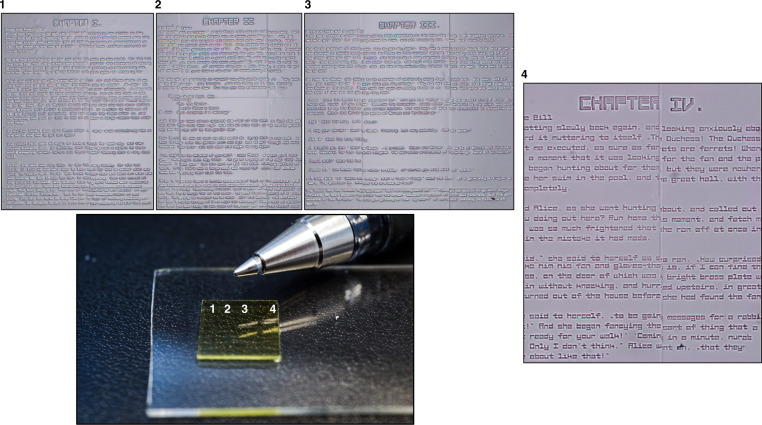
Projection micro stereolithography (PµSL) is a digital light processing (DLP) based printing technique for producing structured microparts. In this approach there is often a tradeoff between the largest object that can be printed and the minimum feature size, with higher resolution generally reducing the overall extent of the structure. The ability to produce structures with high spatial resolution and large overall volume, however, is immensely important for the creation of hierarchical materials, microfluidic devices and bioinspired constructs. In this work, we report a low-cost system with 1 µm optical resolution, representing the highest resolution system yet developed for the creation of micro-structured parts whose overall dimensions are nevertheless on the order of centimeters. To do so, we examine the limits at which PµSL can be applied at scale as a function of energy dosage, resin composition, cure depth and in-plane feature resolution. In doing so we develop a unique exposure composition approach that allows us to greatly improve the resolution of printed features. This ability to construct high-resolution scalable microstructures has the potential to accelerate advances in emerging areas, including 3D metamaterials, tissue engineering and bioinspired constructs.

Keywords: Engineering; Optical materials and structures.


Conflict of interest statement

Conflict of interestThe authors declare no competing interests.

Figures

Fig. 1
Fig. 1. Large Area Micro-Printer (LAMP) system.
a Schematic diagram of the optical and mechanical components of the ultra-resolution, 1 µm pixel size LAMP system. The XY scanning system traverses across the whole DLP and illumination assembly below the micro vat. b Model of the fully enclosed LAMP system. c Rendered model of the Melbourne central business district showing how the LAMP system segments large volumes into smaller sub-projections
Fig. 2
Fig. 2. Development of exposure compensation approach.
a Illustration of how the LAMP exposure compensation algorithm automatically segments regions of a given layer based on feature size. b Relationship between NPS concentration, exposure time and penetration depth. Black squares represent the measured data locations, the contour plot has been linearly interpolated between these locations to build a complete parameter space. c Array of circular features ranging from 20 → 1 μm (left to right) are projected without exposure compensation. Insert shows a HIM image of the test structure, with the white box indicating the region of unresolved features in the 10 → 1 μm range. d Exposure time represented as a function of feature size. White squares represent recorded data locations, black squares indicate the recorded approximate 1:1 mapping location. White line is the interpolated 1:1 mapping between the projected feature size and printed feature size based on the black squares. e Array of the same circular features from (c) with exposure compensation enabled. f Distribution plot of the produced in-plane feature size, with and without exposure compensation. Inset shows the maximum feature delta (δ) between the printed object and the projected feature measured in µm
Fig. 3
Fig. 3. Exposure parameters and microscale feature dimensions, and comparison with prior work.
a Line width measurements for 1 μm and 2 μm lines for increasing exposure time. b Helium ion microscopy (HIM) images of projected 2 μm lines imaged from above. c The LAMP printing system contrasted against prior projection micro-stereolithography based systems. Note that LAMP-D denotes the demonstrated maximum voxel number used in this work, evidencing the ability to produce large numbers of voxels at very high resolutions. Arrows below the color bar indicate the print times of select models. From left to right these include the mushrooms (Fig. 5c), benchy (Fig. 4a), CBML logo (Fig. 6b), microstructure array (Fig. 6g), Melbourne model (Fig. 8f) and periodic lattice (Fig. 8a)
Fig. 4
Fig. 4. Importance of pixel size on achieved resolution illustrated using the 3DBenchy torture test.
a 1 μm pixel size, b 5 μm pixel size, c 10 μm pixel size and d 20 μm pixel size. The projected masks for images (bd) have been artificially down-sampled to produce the desired pixel size. Scale bars 100 μm
Fig. 5
Fig. 5. Single-projection (1 × 1 mm) parts.
Parts imaged using DLSR (a) and HIM (bf). a Kelvin-cell lattice imaged next to an Australian 5c coin, scale bar 1 mm. b Array of micropillars 10 μm in diameter and 40 μm tall. Scale bar 50 μm. c Bio-inspired mushroom structures, scale bar 50 μm. d Kelvin-cell lattice as shown in (a), scale bar 100 μm. e Top-down view of gyroid lattice, scale bar 50 μm. d 3DBenchy boat array, scale bar 100 μm
Fig. 6
Fig. 6. Parts produced using a multiple projection field of view.
Parts imaged using DLSR (a, e, g), optical microscope (b) and HIM (c, d, f, g). a CBML lab logo print next to a pair of tweezers, scale bar 5 mm. b CBML lab logo print imaged under optical microscope, scale bar 1 mm. c, d Close-up image of surface topology and stitching error, scale bar 130 μm. e 10 × 5 mm microneedle array, scale bar 10 mm. f Close-up of microneedle array, scale bar 100 μm. g Array of 625 parts in a 10 × 10 mm area, scale bar 10 mm. h Micro-lattice next to an Australian 50c coin, scale bar 10 mm
Fig. 7
Fig. 7. Alice in Wonderland.
Numbered images correspond to different chapters of the Alice in Wonderland text and their associated placement on the 10 × 10 mm print. All text images were imaged using an inverted microscope, with the total text height for each letter being 40 μm
Fig. 8
Fig. 8. Examples of large, multi-stitched geometries.
a 25 mm × 25 mm × 5 mm large periodic lattice with an Australian 50c coin for scale. b HIM of lattice shown in (a) in the region highlighted in white. c Non-periodic acoustic hologram, approximately 15 mm × 15 mm × 3 mm. d Neurovascular model with 100 μm channels containing red and blue dye. e Micro-lattice tensile sample shown against a matchstick. f Model of Melbourne central business district, containing all roads, buildings and bridges

References

    1. Daminabo SC, Goel S, Grammatikos SA, Nezhad HY, Thakur VK. Fused deposition modeling-based additive manufacturing (3D printing): techniques for polymer material systems. Mater. Today Chem. 2020;16:100248. doi: 10.1016/j.mtchem.2020.100248. - DOI
    1. Mohamed OA, Masood SH, Bhowmik JL. Optimization of fused deposition modeling process parameters: a review of current research and future prospects. Adv. Manuf. 2015;3:42–53. doi: 10.1007/s40436-014-0097-7. - DOI
    1. Lewis JA. Direct ink writing of 3D functional materials. Adv. Funct. Mater. 2006;16:2193–2204. doi: 10.1002/adfm.200600434. - DOI
    1. Wan X, Luo L, Liu Y, Leng J. Direct ink writing based 4D printing of materials and their applications. Adv. Sci. 2020;7:2001000. doi: 10.1002/advs.202001000. - DOI - PMC - PubMed
    1. Huang J, Qin Q, Wang J. A review of stereolithography: processes and systems. Processes. 2020;8:1138. doi: 10.3390/pr8091138. - DOI

Publication types