. 2023 May 30;14(1):3147.
doi: 10.1038/s41467-023-38848-0.

Layered metals as polarized transparent conductors

Affiliations

Layered metals as polarized transparent conductors

Carsten Putzke et al. Nat Commun. .

Abstract

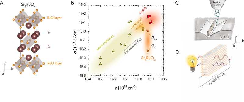
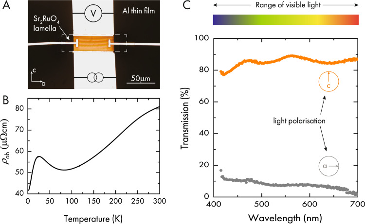
The quest to improve transparent conductors balances two key goals: increasing electrical conductivity and increasing optical transparency. To improve both simultaneously is hindered by the physical limitation that good metals with high electrical conductivity have large carrier densities that push the plasma edge into the ultra-violet range. Technological solutions reflect this trade-off, achieving the desired transparencies only by reducing the conductor thickness or carrier density at the expense of a lower conductance. Here we demonstrate that highly anisotropic crystalline conductors offer an alternative solution, avoiding this compromise by separating the directions of conduction and transmission. We demonstrate that slabs of the layered oxides Sr2RuO4 and Tl2Ba2CuO6+δ are optically transparent even at macroscopic thicknesses >2 μm for c-axis polarized light. Underlying this observation is the fabrication of out-of-plane slabs by focused ion beam milling. This work provides a glimpse into future technologies, such as highly polarized and addressable optical screens.


Conflict of interest statement

The authors declare no competing interests.

Figures

Fig. 1
Fig. 1. Transparent correlated electron system Sr2RuO4.
A Crystal structure of SRO. Highly conductive RuO-layers are separated by Sr donor atoms. B Electrical conductivity versus carrier density of indium-tin-oxide (ITO, triangle), metals (squares, Ni, Cu, Au, Pd), and correlated metals (circles: SrVO3 and CaVO3 REF; diamonds: SRO),,. For ITO the region of transparent thin film conductors is indicated. For SRO the in-plane (σab) and out-of-plane (σc) conductivity is shown, where σabσc>100. The c-axis conductivity in SRO is found to be similar to that of transparent conductors like ITO. C Schematic illustration of the focused ion beam micro-machining process used to obtain a slab of SRO with the shortest direction along an in-plane lattice vector. D Sketch of the main result found in this work. An in-plane confined ac-slab of SRO is back illuminated by a white light source while simultaneously allowing measurements of the in-plane electrical conductivity. Light in the visible range is transmitted through a macroscopic thickness of SRO.
Fig. 2
Fig. 2. 400 nm thick lamella.
A An optical image of the lamella on sapphire. The resistivity measurement is schematically shown. Resistivity of Sr2RuO4 with in-plane confinement (B). Transmission in the range of visible light is shown in (C). Two different polarization directions were measured. One with linearly polarized light along the planes and one with the light linearly polarized perpendicular to the planes. While in-plane light is mostly absorbed, light polarized out-of-plane is transmitted with more than 80% efficiency.
Fig. 3
Fig. 3. Linear polarizing transparent conductor.
A, C, D Optical microscope images of two slabs of SRO with a thickness of 1 μm each are placed on each other with a parallel orientation. B Schematic of the setup used to demonstrate the linearly polarizing property of SRO. One slab is placed on a patterned Al-thin film on sapphire. A second sample can be placed either parallel (A) or perpendicular (C) to the first slab. Firstly, this demonstrates the transparency of SRO even at macroscopic thicknesses. The linear polarization can be further demonstrated by engaging a polarization filter in the microscope. The orientation of the filter is indicated in each panel. For panel D the filter was set to allow only a-axis polarized light to pass. The EPFL logo visible in panels A and C is absent as the sample only allows c-axis polarized light to pass. The bottom row (E, F) shows the same effect for an ac-slab of Tl2201 for c-polarized light (E) and a-polarized light (F).
Fig. 4
Fig. 4. Mueller Matrix.
A Mueller polarimetry microscope, including white light source (WL), linear polarizers (LP), motorized rotator quarter-wave plates (QWP), microscope objectives (0.55NA, 10 mm working distance, Obj), CCD camera and fiber coupled spectrometer. Micrograph of the SRO slab sample under white light and laser illumination (inset). B Measured wavelength-dependent Mueller matrix coefficients. The solid curves show the data while the dashed line represents the results expected for an ideal linear polarizer. The small deviation from the expected result for an ideal polariser highlights the metrological challenge.

References

    1. Aschroft, N. W. & Mermin, D. N. Solid State Physics (Holt-Saunders, 1976).
    1. Wang Y, Plummer EW, Kempa K. Foundations of plasmonics. Adv. Phys. 2011;60:799–898. doi: 10.1080/00018732.2011.621320. - DOI
    1. Zhang L, et al. Correlated metals as transparent conductors. Nat. Mater. 2016;15:204–210. doi: 10.1038/nmat4493. - DOI - PubMed
    1. Zhang, C., Ji, C., Park, Y. B. & Guo, L. J. Thin-metal-film-based transparent conductors: material preparation, optical design, and device applications. Adv. Opt. Mater. 9, 2001298 (2021).
    1. Mackenzie AP, et al. Hall effect in the two-dimensional metal Sr2RuO4. Phys. Rev. B. 1996;54:7425–7429. doi: 10.1103/PhysRevB.54.7425. - DOI - PubMed