

Elimination of Interface Energy Barriers Using Dendrimer Polyelectrolytes with Fractal Geometry
- PMID: 37269290
- PMCID: PMC10802975
- DOI: 10.1021/acsami.3c01930
Elimination of Interface Energy Barriers Using Dendrimer Polyelectrolytes with Fractal Geometry
Abstract
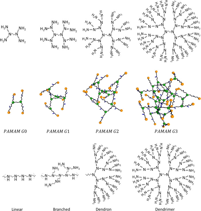
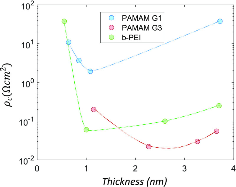
In this work we study conjugated polyelectrolyte (CPE) films based on polyamidoamine (PAMAM) dendrimers of generations G1 and G3. These fractal macromolecules are compared to branched polyethylenimine (b-PEI) polymer using methanol as the solvent. All of these materials present a high density of amino groups, which protonated by methoxide counter-anions create strong dipolar interfaces. The vacuum level shift associated to these films on n-type silicon was 0.93 eV for b-PEI, 0.72 eV for PAMAM G1 and 1.07 eV for PAMAM G3. These surface potentials were enough to overcome Fermi level pinning, which is a typical limitation of aluminium contacts on n-type silicon. A specific contact resistance as low as 20 mΩ·cm2 was achieved with PAMAM G3, in agreement with the higher surface potential of this material. Good electron transport properties were also obtained for the other materials. Proof-of-concept silicon solar cells combining vanadium oxide as a hole-selective contact with these new electron transport layers have been fabricated and compared. The solar cell with PAMAM G3 surpassed 15% conversion efficiency with an overall increase of all the photovoltaic parameters. The performance of these devices correlates with compositional and nanostructural studies of the different CPE films. Particularly, a figure-of-merit (Vσ) for CPE films that considers the number of protonated amino groups per macromolecule has been introduced. The fractal geometry of dendrimers leads to a geometric increase in the number of amino groups per generation. Thus, investigation of dendrimer macromolecules seems a very good strategy to design CPE films with enhanced charge-carrier selectivity.
Keywords: Fermi-level pinning; conjugated polyelectrolytes; dendrimer; dipole; dipole film; electronic transport; solar cells.
Conflict of interest statement
The authors declare no competing financial interest.
Figures


References
-
- Richter A.; Glunz S. W.; Werner F.; Schmidt J.; Cuevas A. Improved Quantitative Description of Auger Recombination in Crystalline Silicon. Phys. Rev. B 2012, 86, 16520210.1103/PhysRevB.86.165202. - DOI
-
- Yan D.; Cuevas A. Empirical Determination of the Energy Band Gap Narrowing in P+ Silicon Heavily Doped with Boron. J. Appl. Phys. 2014, 116, 19450510.1063/1.4902066. - DOI
-
- Yan D.; Cuevas A. Empirical Determination of the Energy Band Gap Narrowing in Highly Doped N+ Silicon. J. Appl. Phys. 2013, 114, 04450810.1063/1.4816694. - DOI
-
- Baker-Finch S. C.; McIntosh K. R.; Yan D.; Fong K. C.; Kho T. C. Near-Infrared Free Carrier Absorption in Heavily Doped Silicon. J. Appl. Phys. 2014, 116, 06310610.1063/1.4893176. - DOI
-
- Holman Z. C.; Descoeudres A.; Barraud L.; Fernandez F. Z.; Seif J. P.; De Wolf S.; Ballif C. In Current Losses at the Front of Silicon Heterojunction Solar Cells, IEEE Journal of Photovoltaics, 2012; Vol. 2 (1), pp 7–1510.1109/JPHOTOV.2011.2174967. - DOI
LinkOut - more resources
Full Text Sources
Research Materials
Miscellaneous
