Review
. 2023 May 23;16(11):3917.
doi: 10.3390/ma16113917.

Functional Materials for Fabrication of Carbon-Based Perovskite Solar Cells: Ink Formulation and Its Effect on Solar Cell Performance

Affiliations
Review

Functional Materials for Fabrication of Carbon-Based Perovskite Solar Cells: Ink Formulation and Its Effect on Solar Cell Performance

Dena Pourjafari et al. Materials (Basel). .

Abstract

Perovskite solar cells (PSCs) have rapidly developed into one of the most attractive photovoltaic technologies, exceeding power conversion efficiencies of 25% and as the most promising technology to complement silicon-based solar cells. Among different types of PSCs, carbon-based, hole-conductor-free PSCs (C-PSCs), in particular, are seen as a viable candidate for commercialization due to the high stability, ease of fabrication, and low cost. This review examines strategies to increase charge separation, extraction, and transport properties in C-PSCs to improve the power conversion efficiency. These strategies include the use of new or modified electron transport materials, hole transport layers, and carbon electrodes. Additionally, the working principles of various printing techniques for the fabrication of C-PSCs are presented, as well as the most remarkable results obtained from each technique for small-scale devices. Finally, the manufacture of perovskite solar modules using scalable deposition techniques is discussed.

Keywords: inkjet printing; metal oxides; nanoinks; nanomaterials; screen printing; spray deposition.


Conflict of interest statement

The authors declare no conflict of interest.

Figures

Figure 1
Figure 1
Energy band diagram of various metal oxides used in perovskite solar cells with carbon electrode. Reproduced with permission from Ref. [8].
Figure 2
Figure 2
Conventional PSC (left) and C-PSC (right) working principles upon light illumination. Efn and Efp represent the electron and hole quasi-Fermi levels, respectively. Reproduced with permission from Ref. [11].
Figure 3
Figure 3
Schematic view of the spin coating stages (ω is the angular velocity).
Figure 4
Figure 4
(a) X-ray diffraction pattern; (b) Raman spectrum with inset of SEM image of brookite nanorods and TEM image of brookite nanocubes; (c) EQE of the champion devices comparing brookite nanorods and nanocubes with commercial anatase; and (d) IS representation along with the fitted electrical circuit diagrams. Reproduced with permission from Ref. [63].
Figure 5
Figure 5
SEM images of (a) CsPbIBr2 cell based on F–SnO2 film; (b) CsPbIBr2 cell based on NP-SnO2 film; (c) cross section of CsPbIBr2 film based on F–SnO2 film; (d) cross section of CsPbIBr2 cell based on NP-SnO2 film; (e) CsPbIBr2 based on F–SnO2 film; (f) the light path in the CsPbIBr2 cell based on NP-SnO2 film. Reproduced with permission from Ref. [67].
Figure 6
Figure 6
Schematic view of the contact angles of ZnO NPs solution dropped on FTO substrates with DI treatment and without DI treatment and the contact angles of the perovskite precursor solution dropped on ZnO/FTO films with and without DI treatment.
Figure 7
Figure 7
XRD spectra of the CsPbBr3 films prepared on different ETLs with corresponding SEM image of CsPbBr3 film grown on Nb2O5/FTO and Li: Nb2O5/FTO. Reproduced with permission from Ref. [74].
Figure 8
Figure 8
Schematic of perovskite cell fabrication processes using different nanomaterials dispersed in the perovskite layer. (a) B-MWNTs on PbI2 layer followed by MAPbI3 perovskite film, reprinted with permission from [78]; Copyright {2017} American Chemical Society. (b) CNPs dispersed in the antisolvent as chlorobenzene; reproduced with permission from Ref. [79].
Figure 9
Figure 9
(a) CQDs dispersed in the antisolvent as ethyl acetate, (b) XPS spectra of EACQDs, (c) deconvolution of C, and (d) XRD image of pristine and 0.01 EACQDs optimized PSCs, reproduced with permission from Ref. [80].
Figure 10
Figure 10
Schematic illustration of the basic principles of screen printing. Reproduced with permission from Ref. [82].
Figure 11
Figure 11
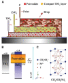
(A) Scheme of fully printable triple-stack mesoporous carbon-based perovskite solar cells (PSC), (B) Band gap diagram of each layer present in the carbon-based PSC, and (C) crystalline structure of MAPbI3 perovskite. Reproduced with permission from Ref. [86].
Figure 12
Figure 12
(A) Implementation of an extra Al2O3 layer with m-TiO2 and m-ZrO2 via a vacuum technique, (B) infiltration of perovskite precursor solution through the layers, and (C) energy band diagram of hole-conductor-free C-PSC with Al2O3 interlayer. Reproduced with permission from Ref. [96].
Figure 13
Figure 13
XRD analyses of black NiOx acquired from Sigma-Aldrich: (a) powder of NiO, Ni(OH)2, NiOOH, and Ni2O3, and (b) mixture of Ni2+ and Ni3+.Reproduced with permission from [98].
Figure 14
Figure 14
Cross-section of the perovskite/triple-stack mesoporous carbon-based solar cell with Co2O3 hole-transporting layer: (a) low magnification, and (b) high magnification, (c) J-V characteristics of standard carbon cell with an aperture area of 0.09 cm2 (under 1 Sun) without and with Co3O4 layer, and (d) J-V characteristics of module with an active area of 70 cm2 and with Co3O4. Reproduced with permission from Ref. [97].
Figure 15
Figure 15
Construction of the: (a) single carbon electrode composed of a mesoporous carbon layer, and (b) double-layer carbon electrode composed of a mesoporous carbon below a conductor carbon layer. Reproduced with permission from Ref. [105].
Figure 16
Figure 16
Working principles of inkjet printers: (a) CIJ; and (b) DOD. Reproduced with permission from Ref [124].
Figure 17
Figure 17
X-ray diffraction (XRD) patterns after infiltrating of CH3NH3PbI3 (MAPI) and annealing. The dominating (101) reflection at 2θ = 25.3° is attributed to anatase TiO2 (inset). At reduced intensity scale, the characteristic reflections of the cubic phase of the MAPI perovskite crystal are clearly visible (blue squares). The absence of a reflection peak at 2θ = 12.5° reveals that all the precursor ink has been transformed to the hybrid metal halide perovskite and that no un-desirable PbI2 is present. Reproduced with permission from Ref. [135].
Figure 18
Figure 18
Schematic illustration of the main components in a slot-die processing set-up.
Figure 19
Figure 19
Schematic illustration of the “doctor blade” film deposition process.
Figure 20
Figure 20
UV-Vis absorbance spectra of ZrO2 film (N_ZrO2) and double-layered film (DL_ZrO2) deposited on glass. Reproduced with permission from Ref. [145].
Figure 21
Figure 21
Schematic illustration of the spray coating deposition process.
Figure 22
Figure 22
(a) Performance of 70 cm2 mini-module with CsBr-modified TiO2 layer in comparison with a standard carbon-based perovskite solar cell; (b) Image of a fully printable mini-module. Reproduced with permission from Ref. [4].

References

    1. Kojima A., Teshima K., Shirai Y., Miyasaka T. Organometal Halide Perovskites as Visible-Light Sensitizers for Photovoltaic Cells. J. Am. Chem. Soc. 2009;131:6050–6051. doi: 10.1021/ja809598r. - DOI - PubMed
    1. Lin Q., Armin A., Burn P.L., Meredith P. Organohalide Perovskites for Solar Energy Conversion. Acc. Chem. Res. 2016;49:545–553. - PubMed
    1. Stefanelli M., Vesce L., Di Carlo A. Upscaling of Carbon-Based Perovskite Solar Module. Nanomaterials. 2023;13:313. - PMC - PubMed
    1. Keremane K.S., Prathapani S., Haur L.J., Bruno A., Priyadarshi A., Adhikari A.V., Mhaisalkar S.G. Improving the Performance of Carbon-Based Perovskite Solar Modules (70 cm2) by Incorporating Cesium Halide in Mesoporous TiO2. ACS Appl. Energy Mater. 2021;4:249–258. doi: 10.1021/acsaem.0c02213. - DOI
    1. Best Research-Cell Efficiency Chart|Photovoltaic Research|NREL. [(accessed on 26 March 2023)]; Available online: https://www.nrel.gov/pv/cell-efficiency.html.

LinkOut - more resources