. 2023 Jun 30;15(25):10808-10819.
doi: 10.1039/d3nr01051a.

Chitosan-gated organic transistors printed on ethyl cellulose as a versatile platform for edible electronics and bioelectronics

Affiliations

Chitosan-gated organic transistors printed on ethyl cellulose as a versatile platform for edible electronics and bioelectronics

Alina S Sharova et al. Nanoscale. .

Erratum in

Abstract

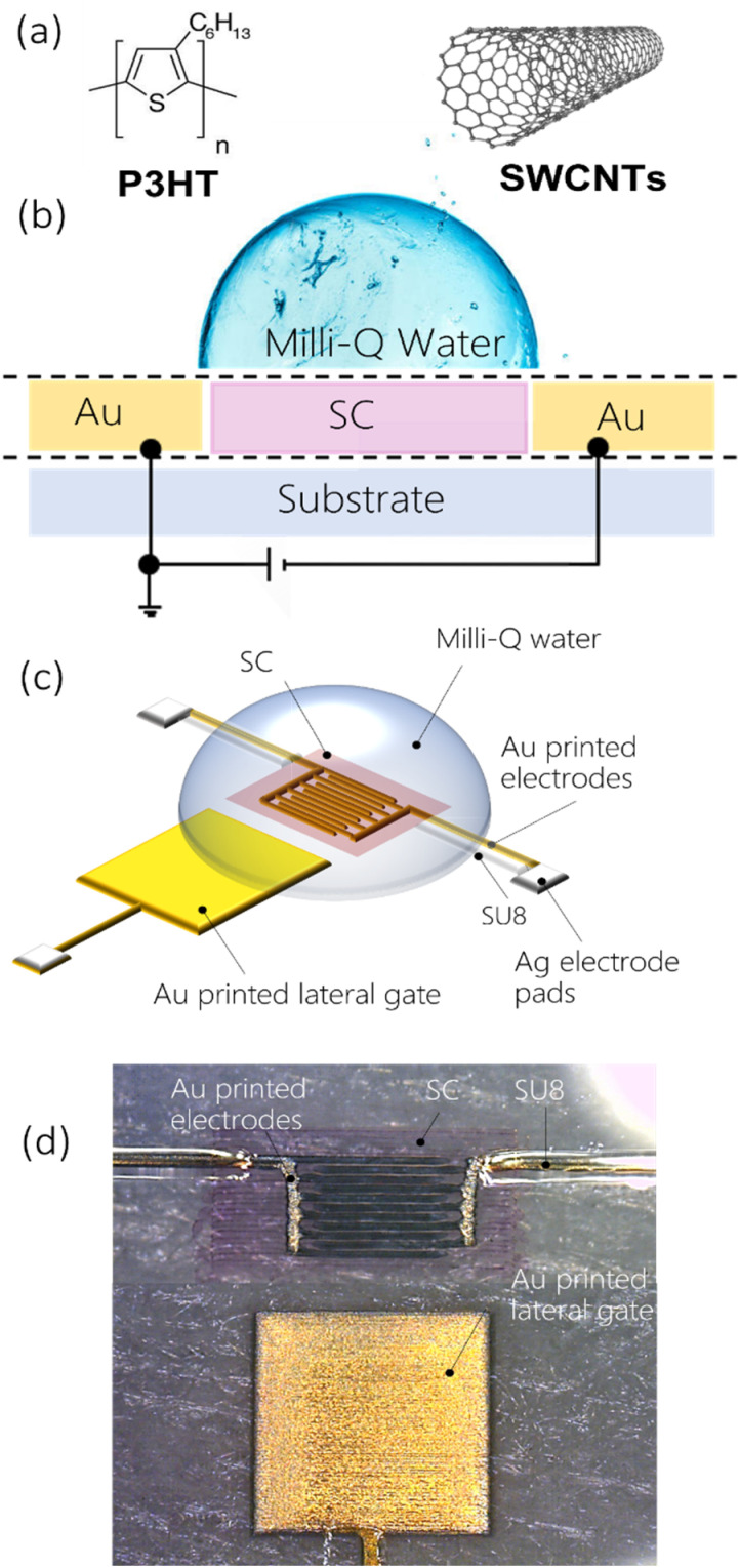
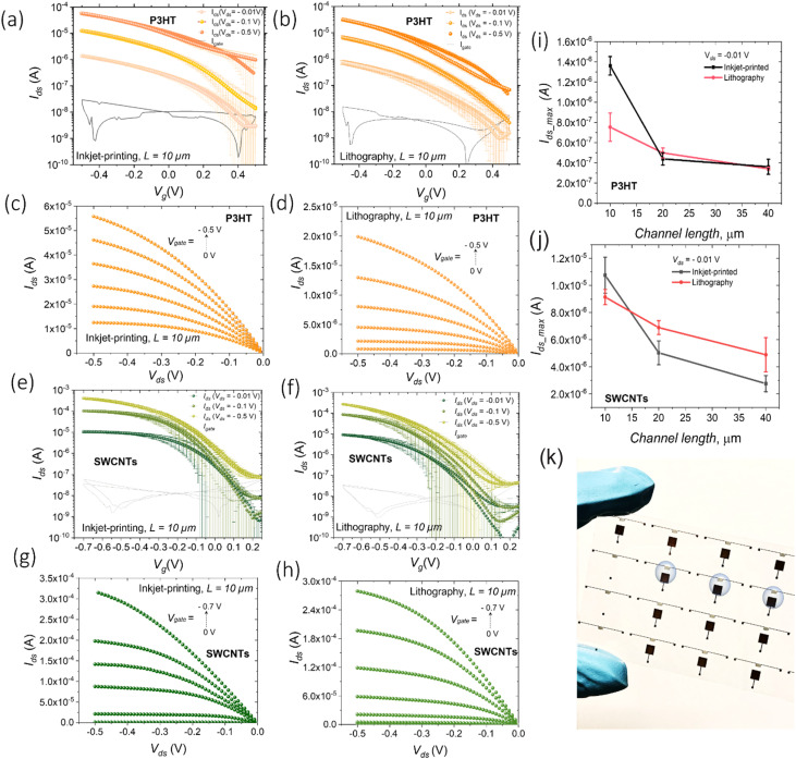
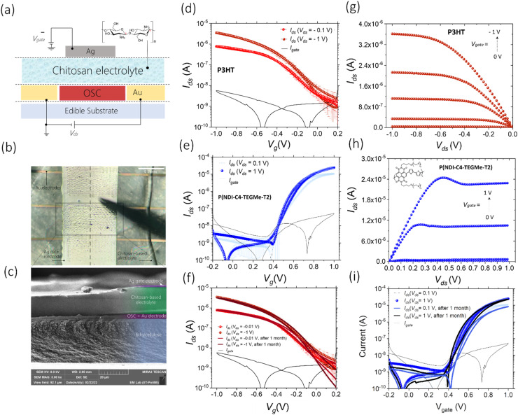
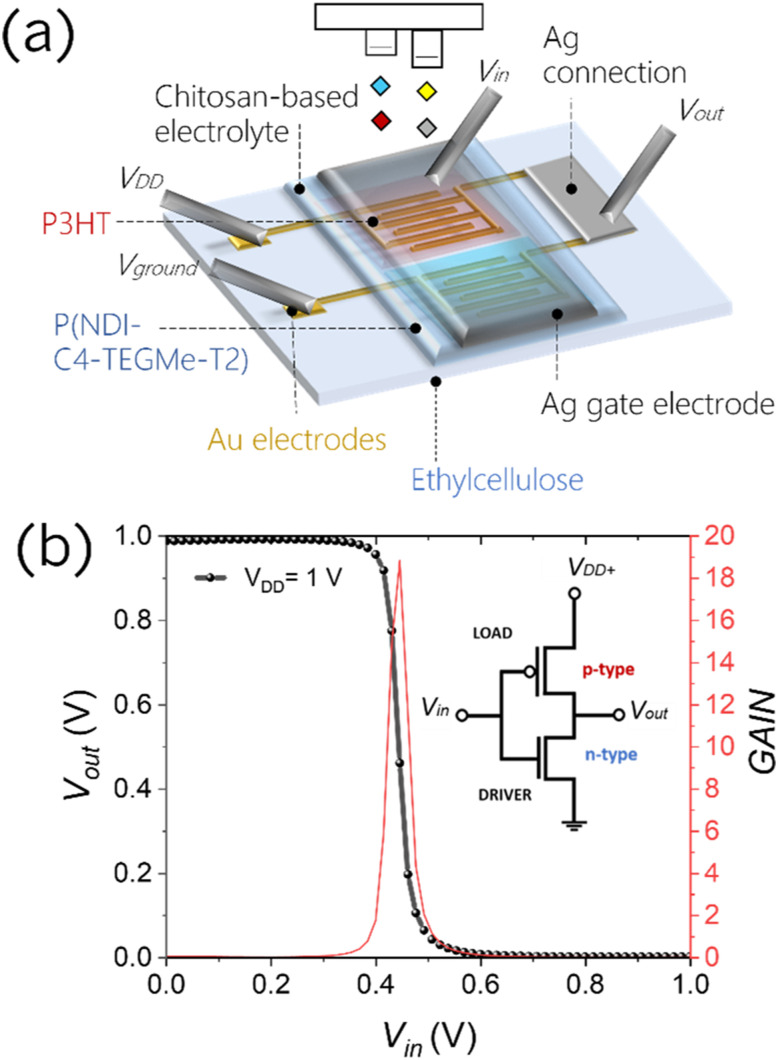
Edible electronics is an emerging research field targeting electronic devices that can be safely ingested and directly digested or metabolized by the human body. As such, it paves the way to a whole new family of applications, ranging from ingestible medical devices and biosensors to smart labelling for food quality monitoring and anti-counterfeiting. Being a newborn research field, many challenges need to be addressed to realize fully edible electronic components. In particular, an extended library of edible electronic materials is required, with suitable electronic properties depending on the target device and compatible with large-area printing processes, to allow scalable and cost-effective manufacturing. In this work, we propose a platform for future low-voltage edible transistors and circuits that comprises an edible chitosan gating medium and inkjet-printed inert gold electrodes, compatible with low thermal budget edible substrates, such as ethylcellulose. We report the compatibility of the platform, characterized by critical channel features as low as 10 μm, with different inkjet-printed carbon-based semiconductors, including biocompatible polymers present in the picogram range per device. A complementary organic inverter is also demonstrated with the same platform as a proof-of-principle logic gate. The presented results offer a promising approach to future low-voltage edible active circuitry, as well as a testbed for non-toxic printable semiconductors.


Conflict of interest statement

The authors declare no conflict of interest.

Figures

Fig. 1
Fig. 1. Structural, morphological, and electrical characterization of inkjet printed gold electrodes on different conventional and edible substrates. (a)–(d) Gold interdigitated electrodes inkjet printed on different substrates: PEN, glass, edible ethyl cellulose and tattoo paper substrates. (g) and (h) Digital photographs of gold electrodes transferred onto different surfaces: (top) a peach, an apple and (bottom) a fingertip. (e) AFM of gold electrodes inkjet printed on PEN: topography of the area between the two conducting fingers of interdigitated electrodes with a channel length of 10 μm; the area of the image is 20 × 20 μm2. (f) AFM topographic image of the top surface of the gold electrode. The image area is 5 × 5 μm2. (i) Dependence of the electrical resistance of inkjet printed gold lines under drying conditions. The plots are presented for lines with a length of 7.5 mm. Each point corresponds to an average value measured over 7 samples.
Fig. 2
Fig. 2. (a) Chemical structure of the semiconducting materials used (P3HT and SWCNTs). (b) Schematic cross-section and (c) representation of a fully printed WGFET. (d) Microscopy image of the device on a PEN substrate.
Fig. 3
Fig. 3. Electrical characterization of WGFETs. (a) Transfer and (c) output characteristic curves of P3HT-based WGFETs with inkjet printed gold electrodes, and (b) transfer and (d) output curves of devices with photolithographically patterned gold electrodes in linear (Vds = −0.01 V; −0.1 V) and saturation (Vds = −0.5 V) regimes; the Vgate sweep rate was 10 mV s−1; transfer curves are averaged over 7 samples; geometrical parameters of WGFETs: L = 10 μm; W = 105 μm. (i) Comparison of max Ids values for two different configurations of P3HT-based WGFETs (based on inkjet printed and photolithographically patterned gold electrodes) in the linear regime (Vds = −0.01 V) for devices with different channel lengths: L = 10 μm, L = 20 μm, and L = 40 μm. (e) Transfer and (g) output characteristic curves of s-SWCNT-based WGFETs, with inkjet printed gold electrodes, and (f) transfer and (h) output curves for devices with photolithographically patterned gold electrodes in linear (Vds = −0.01 V; −0.1 V) and saturation (Vds = −0.5 V) regimes; the Vgate sweep rate was 10 mV s−1; transfer curves are averaged over 7 samples; geometrical parameters of OFETs: L = 10 μm; W = 105 μm. (j) Comparison of max Ids values for two different configurations of s-SWCNT-based WGFETs (based on inkjet printed and photolithographically patterned gold electrodes) in the linear regime (Vds = −0.01 V) for the devices with different channel lengths: L = 10 μm, L = 20 μm, and L = 40 μm. (k) A digital image of WGFETs.
Fig. 4
Fig. 4. Structure, fabrication, and electrical characterization of fully printed chitosan-gated transistors on an edible substrate. (a) Schematic structural representation of the device. Chemical structure of chitosan is shown in the inset. (b) Microscopy image of three fully printed chitosan-gated transistors on an ethylcellulose substrate with a common silver gate electrode (top view). The dashed line indicates the cross-section imaged via SEM (c). It is possible to distinguish the layers composing the device: an ethylcellulose substrate (30 μm), a layer of a semiconductor deposited on the gold source and drain electrodes, a chitosan-based electrolyte (15 μm), and a silver gate electrode. The layer of the semiconducting polymer was printed approximately 10 times thicker than in the actual device to help distinguish it in the stack with other layers. (d) Transfer and (e) output characteristic curves of fully printed p-type chitosan-gated transistors on an ethylcellulose substrate in linear (Vds = −0.1 V) and saturation (Vds = −1 V) regimes (average curve over 7 samples); the Vgate sweep rate was 5 mV s−1. (f) Transfer and (g) output characteristic curves of fully printed n-type chitosan-gated transistors on an ethylcellulose substrate in linear (Vds = 0.1 V) and saturation (Vds = 1 V) regimes (average curve over 7 samples); the Vgate sweep rate was 2 mV s−1. Shelf-life stability of fully printed (h) p-type and (i) n-type chitosan-gated transistors. A comparison between electronic performances (transfer characteristics in linear and saturation regimes) after a 1-month control period of storing the devices in air is shown.
Fig. 5
Fig. 5. (a) Schematic representation of the inverting logic gate device realized with chitosan-gated transistors based on P3HT and P(NDI-C4-TEGMe-T2); L = 10 μm and W = 10 000 μm for the p-type device and L = 30 μm and W = 10 000 μm for the n-type device. (b) Complementary inverter voltage transfer curve (VTC) and the corresponding derivative curve to extract gain as a function of input voltages; the sweep rate is 15 mV s−1; the inverter configuration is given as an inset.

Similar articles

Cited by

References

    1. Kanaparthi S. Badhulika S. Solvent-free fabrication of biodegradable all-carbon paper based Field Effect Transistor for human motion detection through strain sensing. Green Chem. 2016;18:3640–3646. doi: 10.1039/C6GC00368K. - DOI
    1. Irimia-Vladu M. et al., Biocompatible and biodegradable materials for organic field-effect transistors. Adv. Funct. Mater. 2010;20:4069–4076. doi: 10.1002/adfm.201001031. - DOI
    1. Irimia-vladu M. “Green” electronics: biodegradable and biocompatible materials and devices for sustainable future. Chem. Soc. Rev. 2014;43:588–610. doi: 10.1039/C3CS60235D. - DOI - PubMed
    1. Spyropoulos G. D. Gelinas J. N. Khodagholy D. Internal ion-gated organic electrochemical transistor : A building block for integrated bioelectronics. Sci. Adv. 2019;2019:5. - PMC - PubMed
    1. Bettinger C. J. Bao Z. Organic Thin-Film Transistors Fabricated on Resorbable Biomaterial Substrates. Adv. Mater. 2010;22:651–655. doi: 10.1002/adma.200902322. - DOI - PMC - PubMed