Review
. 2023 Jun 20;12(1):152.
doi: 10.1038/s41377-023-01169-4.

Integrated metasurfaces for re-envisioning a near-future disruptive optical platform

Affiliations
Review

Integrated metasurfaces for re-envisioning a near-future disruptive optical platform

Younghwan Yang et al. Light Sci Appl. .

Abstract

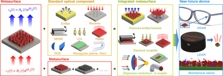
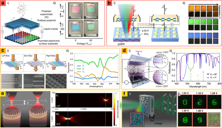
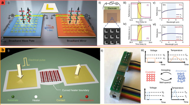
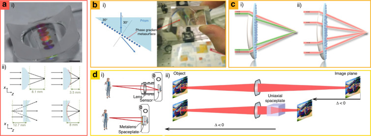
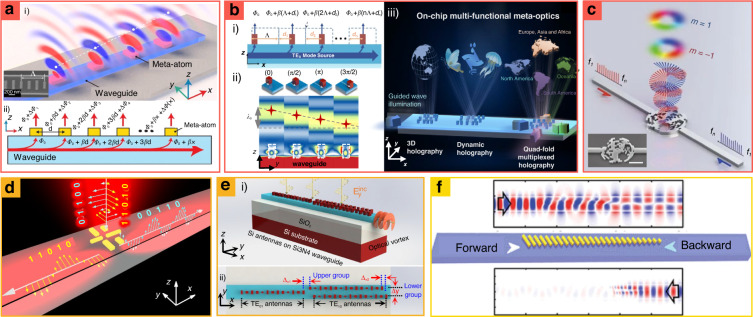
Metasurfaces have been continuously garnering attention in both scientific and industrial fields, owing to their unprecedented wavefront manipulation capabilities using arranged subwavelength artificial structures. To date, research has mainly focused on the full control of electromagnetic characteristics, including polarization, phase, amplitude, and even frequencies. Consequently, versatile possibilities of electromagnetic wave control have been achieved, yielding practical optical components such as metalenses, beam-steerers, metaholograms, and sensors. Current research is now focused on integrating the aforementioned metasurfaces with other standard optical components (e.g., light-emitting diodes, charged-coupled devices, micro-electro-mechanical systems, liquid crystals, heaters, refractive optical elements, planar waveguides, optical fibers, etc.) for commercialization with miniaturization trends of optical devices. Herein, this review describes and classifies metasurface-integrated optical components, and subsequently discusses their promising applications with metasurface-integrated optical platforms including those of augmented/virtual reality, light detection and ranging, and sensors. In conclusion, this review presents several challenges and prospects that are prevalent in the field in order to accelerate the commercialization of metasurfaces-integrated optical platforms.


Conflict of interest statement

The authors declare no competing interests.

Figures

Fig. 1
Fig. 1. Overall concept of metasurface integration and its promising applications.
Recently, metasurfaces have been integrated with standard optical components, such as emitters, receivers, microelectromechanical systems (MEMS), refractive optical elements (ROEs), waveguides, and other metasurfaces. Integrated metasurfaces gain extended functionalities and this will be further applied to a near-future device including virtual reality (VR), augmented reality (AR), light detection and ranging (LiDAR), and bio/chemical sensors
Fig. 2
Fig. 2. Metasurface-integrated light emitters for (a–c) efficiency improvement and (d–f) wavefront shaping.
a.i Schematics and a.ii an SEM image of disordered Ag nanoparticle-integrated GaN emitters. a.iii Electroluminescence (EL) intensity IEL with/without Ag nanoparticles, corresponding to green and red curves, respectively. b Ag metasurface-integrated second harmonic generation (SHG) emitters. cMQWs: coupled multiple quantum wells. Red arrow: incident direction of a pump laser. c.i Schematic of meta mirror-integrated organic light emitting diodes (LEDs). c.ii SEM and c.iii optical microscope image of the meta mirror. c.iv Luminescence intensity comparison of meta mirror-integrated and color-filtered organic LEDs, corresponding to solid and dashed curves, respectively. d.i Schematics of metasurface-integrated vertical-cavity surface-emitting lasers (VCSELs), and d.ii its Bessel beam generation. DBRs: distributed Bragg reflector mirrors. d.iii Measured intensity profiles of the Bessel beam along the propagation direction. e.i Schematic of InGaN/GaN quantum-well metasurfaces for unidirectional luminescence. e.ii SEM images of fabricated InGaN/GaN quantum-well metasurfaces. f.i Meta-atom of MQW-comprised metasurface SHG emitters. f.ii Magnitude of χ(2) as a function of the pump wavelengths depending on bias voltages. f.iii Schematic of metasurface-integrated nonlinear emitters with various artificial structures. f.iv Depending on grating patterns and bias voltages, the propagation direction of the emitted light is adjusted. a is reproduced with permission from Ref. Copyright © 2021, Peng Mao et al., b from ref. Copyright © 2019 Haoliang Qian, et al., c from ref. . Reprinted with permission from AAAS, d from ref. Copyright © 2020 Springer Nature, e from ref. Copyright © 2020 Springer Nature, f from ref. Copyright © 2020 The Springer Nature
Fig. 3
Fig. 3. Metasurface-integrated single-photon emitters with (a) β-barium borate (BBO) crystals, (b) nitrogen-vacancy (NV) centered diamonds, and (c and d) 2D materials.
a.i Schematic and a.ii optical microscopy image of metasurface-integrated spontaneous photon-emitter. b.i Schematics of HSQ metasurface-integrated single-photon emitter. A yellow dot at the bottom schematic presents the NV-centered diamond with b.ii right-circularly polarized (RCP) and b.iii left-circularly polarized (LCP) light emitters have been demonstrated. The hydrogen silsesquioxane (HSQ) metasurface consists of an azimuthally gradient width. c.i SEM image of metasurfaces before 2D emitter integration. c.ii Fabrication process of metasurface-integrated 2D emitter. LM: layered materials. PDMS: polydimethylsiloxane. c.iii Dark field optical microscopy images of the metasurface-integrated 2D emitters. Blue and red circles: positions of pierced and non-pierced 2D materials, respectively. d.i Schematic and d.ii SEM images of plasmonic nanocavity integrated 2D emitters. d.iii Time-resolved photoluminescence (PL) measurement for comparison of emission rate between conventional (pristine emitter) and plasmonic nanocavity integrated 2D emitters (coupled emitter). a is reproduced with permission from ref. . Reprinted with permission from AAAS, b from ref. Copyright © 2020 Wiley-VCH, c from ref. Copyright © 2017 Carmen Palacios-Berraquero et al., d from ref. Copyright © 2017 American Chemical Society
Fig. 4
Fig. 4. Metasurfaces-integrated receivers for (a and b) efficiency improvement, (c) selective photodetection, (d and e) wavefront sorting, and (f) increasing field of view (FoV).
Efficiencies of a UV and b RGB charge-coupled devices (CCDs) have been improved by integrating metalenses. Compared to a.i, and b.i CCDs without metalenses, a.ii and b.ii metalens-integrated CCDs achieve higher efficiencies by focusing the incident light on the photosensitive area. c.i Schematics of metasurface-integrated hybrid organic–inorganic perovskites (HOIPs) for optoelectronic devices. Metasurface-integrated HOIPs consist of c.ii HOIP meta-atoms and c.iii backplane mirrors. d.i Schematics of metasurface-integrated CCD for orbital angular momentum (OAM) sorting. d.ii Focal point of the metasurfaces depends on the topological charge of OAM. e.i Schematics of computation systems with the metasurface-integrated CCD. e.ii Depending on the incident wavefront, the focusing points of outgoing light from metasurface-integrated CCDs are varied. f Wide FoV with a multiple aperture-integrated CCD. a is reproduced with permission from ref. Copyright © 2021 American Chemical Society, b from ref. Copyright © 2022, Xiujuan Zou et al., c from ref. Copyright © 2022 American Chemical Society, d from ref. Copyright © 2022 American Chemical Society. e from ref. Copyright © 2022 Xuhao Luo et al., f from ref. Copyright © 2022, Li Zhang et al.
Fig. 5
Fig. 5. Microelectromechanical systems (MEMS)-integrated metasurfaces for MEMS-actuated (a and b) metalens, (c) beam-steerer and (d and e) structural-color pixel.
a Tunable dielectric doublet metalens using the MEMS-based SiNx membrane. a.i Illustration of the operation principle and design. a.ii SEM images of the doublet lens system on (top) the metasurface on the membrane and (bottom) its nanostructures (scale bars: 100, 1 μm). b Adaptive metalens which can simultaneously control focal length, astigmatism, and shift. b.i Device design of the dielectric elastomer metalens comprising the five reconfigurable voltage connections. b.ii Experimental focal shifts using the middle electrode V5. Solid blue lines, blue circles, and red triangles represent the fit of focal points, focal length, and stretch, respectively, as a function of the applied voltage. c Dynamic beam steering device based on the integration of optical metasurfaces and piezoelectric MEMS mirror. c.i Operational schemes for 2D wavefront shaping of the device, specular reflection, and c.ii anomalous reflection. c.iii Image of monolithic integration between MEMS mirror and optical metasurfaces. c.iv Optical microscope images and c.v SEM images of the 30 × 30 μm2 metasurface and 250 nm-period gold meta-atoms in the MEMS-mirror-based dynamic beam steering device. d Temporal color mixing device obtained by modulating the gap between two Si layers. d.i Dynamic height control of MEMS-integrated tunable temporal color mixing device from 0 to 2.75 V. d.ii Mechanical simulation by changing voltages and Sin thicknesses (pixel size: 12 μm). d.iii Bright-field images of tunable color pixels consist of nanowires. Scale bar: 2 μm. d.iv Temporally combined colors by the diverse electric duty cycle. e Transmissive adjustable color filters combined with MEMS cantilever. e.i Schematic of the design and principle. Transmission can be controlled by a MEMS cantilever. e.ii SEM images of MEMS cantilever (scale bar: 50 μm) and e.iii SEM and optical microscope images of plasmonic nanohole arrays corresponding transmission colors (scale bars: 250 nm to SEM images and 30 μm to microscope images). a is reproduced with permission from ref. Copyright © 2018, Ehsan Arbabi et al., b from ref. Copyright © 2018 The Authors, some rights reserved; exclusive licensee American Association for the Advancement of Science, Distributed under a CC BY-NC 4.0 license http://creativecommons.org/licenses/by-nc/4.0/, Reprinted with permission from AAAS, c from ref. Copyright © 2021 The Authors, some rights reserved; exclusive licensee American Association for the Advancement of Science, Distributed under a CC BY-NC 4.0 license http://creativecommons.org/licenses/by-nc/4.0/, Reprinted with permission from AAAS, d from ref. Copyright © 2019 The American Association for the Advancement of Science, e from ref. Copyright © 2022 The Authors, some rights reserved; exclusive licensee, Distributed under a CC BY-NC 4.0 license http://creativecommons.org/licenses/by-nc/4.0/, Reprinted with permission from AAAS American Association for the Advancement of Science
Fig. 6
Fig. 6. Liquid crystal (LC)-integrated metasurfaces for tunable (a and b) structural color pixel, (c and d) spatial light modulator (SLM), and (e and f) metalens and metahologram.
a Plasmonic metadisplay composed of addressable structural color using single pixel. a.i Schematic of the polarization-dependent full-color pixel design. The ambient white light passes through a polarizer and LC and the plasmonic metasurfaces serve as polarization-dependent absorbers, resulting in different colors reflection. a.ii Captured images of the LC-powered plasmonic device depending on incident polarization. Pixel size: 1 × 1 inch2. b All-dielectric metasurfaces integrated with LC for dynamic colors. b.i Schematics of operational principle. b.ii Optical microscope images of the full-color gradients by controlling linear polarizer axis from 0° to 90°. Pixel size: 100 × 100 μm2. c Phase-only SLM device based on LC-integrated metasurfaces. c.i Drawings of the design and SEM images of fabricated SLM. Scale bars: 5 μm, 600 nm and 250 nm. c.ii Measured transmission at three diffraction orders. d LC-coupled SLM based on Fabry–Perot nanocavities. d.i Illustrations of the device. d.ii Simulated reflectance as a function of wavelength, according to two different LC orientation angles (0° and 90°). e Electrically controlled bifocal metalens. e.i Schematic of bifocal metalens. The focal lengths are shifted by applying a different electrical voltage. e.ii The measured focusing intensity profiles at the x–z plane with different incident light, left-circularly polarized (LCP), and e.iii right-circularly polarized light (RCP). f Bifunctional metasurfaces integrated with LC analyzer. f.i Schematic of the device. f.ii Different metahologram images were obtained by applying different electrical bias and optical microscope images of a quick response code. a is reproduced with permission from ref. Copyright © 2017, Daniel Franklin et al., b from ref. Copyright © 2022, Trevon Badloe et al., c from ref. , Reprinted with permission from AAAS, d from ref. Copyright © 2022, Shampy Mansha et al., e from ref. Copyright © 2021 Badloe, T. et al. Advanced Science published by Wiley‐VCH GmbH, f from ref. Copyright © 2021, Inki Kim, et al.
Fig. 7
Fig. 7. Heater-integrated metasurfaces that consist of (a) VO2 and (b) Ge2Sb2Se5Te (GSST).
a Electrically tunable VO2 metasurfaces for dynamic phase modulation. a.i Schematics of heater-integrated VO2 metasurfaces. a.ii Heat is induced by electric voltage. The measurement of a.iii heating and a.iv cooling time. a.v and a.vi The optical responses are varied according to the applied electric current on electrodes. b Electrically reconfigurable GSST metasurfaces with a microscale heater. b.i Schematics and b.ii the photo of heater-integrated tunable metasurfaces. b.iii Depending on heating time and temperature, the phase of GSST is varied. Tm: melting point, Tx: crystallization temperature of GSST. a is reproduced with permission from ref. Copyright © 2021 Wiley-VCH, b from ref. Copyright © 2021 Springer Nature
Fig. 8
Fig. 8. Metasurfaces-integrated refractive optical elements for (a) modifying optical function from geometry, (b and c) dispersion control, and (d) miniaturizing.
a.i Metasurfaces-attached concave glass cylinder behaving like converging aspherical lens. a.ii Focal distance of 8.11 mm of a converging cylindrical lens is modified to 3.5 mm. Concave glass cylinders with a focal distance of -12.7 mm behave as an aspherical lens having a focal distance of 8 mm. b.i Schematic of the achromatic system. b.ii Experimentally realized achromatic optical component. Schematic of the c.i chromatic aberration corrected lens and c.ii spherical aberration corrected lens. d.i Standard camera (top) and spaceplate added camera (bottom). d.ii The spaceplate advances the image’s focal plane by -3.4 mm. a is reproduced with permission from ref. Copyright © 2016, Seyedeh Mahsa Kamali et al., b from ref. Copyright © 2019 Wiley-VCH, c from ref. Copyright © 2021 Optica Publishing Group, d from ref. Copyright © 2021 Orad Reshef et al.
Fig. 9
Fig. 9. Metasurfaces-integrated planar waveguides for (a–c) structured light, (d and e) demultiplexing, (f) diode.
a.i Schematic of a guided wave-driven metasurface and a.ii wavefront formation of the extracted wave. b.i Schematic of a wavefront formation with imparting. b.ii Simulated electric field distribution (Ey) for the phase shift of 0, π/2, π, and 3π/2. b.iii Schematic illustrating novel on-chip meta-holography applications, including multiplane 3D holography, dynamic holography, and quad-fold multiplexed holography. c Schematic of the broadband multiplexed OAM emitter. d Waveguide-integrated plasmonic nanoantenna that enables mode-selective polarization (de)multiplexing. e.i Schematic of the chip-integrated orbital angular momentum generator and e.ii its top view. f Gradient metasurface on the waveguide inducing asymmetric transmission. a is reproduced with permission from ref. Copyright © 2020 The Authors, some rights reserved; exclusive licensee American Association for the Advancement of Science, Distributed under a CC BY-NC 4.0 license http://creativecommons.org/licenses/by-nc/4.0/, Reprinted with permission from AAAS, b from ref. Copyright © 2022 Wiley-VCH, c from ref. Copyright © 2018, Zhenwei Xie et al., d from ref. Copyright © 2017 The Authors, some rights reserved; exclusive licensee American Association for the Advancement of Science, Distributed under a CC BY-NC 4.0 license http://creativecommons.org/licenses/by-nc/4.0/, Reprinted with permission from AAAS, e from ref. Copyright © 2020 Optica Publishing Group, f from ref. Copyright © 2019 American Chemical Society
Fig. 10
Fig. 10. Metasurface-integrated fibers for (a) filtering, (b) steering, (c) focusing, (d) imaging, and (e) sensing.
a.i SEM images of nanopatterned fiber for polarization-sensitive optical response. a.ii Polarization-sensitive transmittance spectra of the fiber. b Metasurface-integrated fiber for beam-steering. c.i Schematic of the achromatic metalens-integrated fiber for focusing telecommunication range. c.ii Experimentally measured point-spread functions of the metafiber. Left: longitudinal planes. Right: transverse planes at five different wavelengths. d.i Schematic (left) and photographic image (right) of the metasurface-integrated fiber for tomography. d.ii Measured focal spot profiles using a graded index (GRIN) optical coherence tomography (OCT) catheter, a ball lens catheter, and the nano-optic endoscope at 1310 nm wavelength. Nano-optic endoscope shows smaller astigmatism. d.iii Ex vivo human lung resections (first, second, and third line) and in vivo in the upper airways of a sheep (fourth line) endoscopic imaging using the nano-optic endoscope. Structural features are clearly visible. e.i SEM images of fabricated metasurface-integrated fiber for chemical sensing. e.ii Illustrative drawing of the biological protocol. e.iii Real-time wavelength shift of the phase-gradient optical fiber meta-tip. a is reproduced with permission from ref. , © 2022 Indra Ghimire et al., published by De Gruyter, Berlin/Boston, b from ref. Copyright © 2022 American Chemical Society, c from ref. Copyright © 2022, Haoran Ren et al., d from ref. Copyright © 2018 Springer Nature, e from ref. Copyright © 2020 Wiley-VCH
Fig. 11
Fig. 11. Optical platform of composed metasurfaces for (a-c) wavelength decoupling, (d and e) polarization decoupling, (f and g) dispersion control, and (h and i) tunability.
a Photonic encryption platform that is composed of ultraviolet and visible metasurfaces. b Bilayer metasurfaces independently control two infrared frequencies. c Composed non-local metasurfaces. c.i Schematics of composed non-local metalenses operating with different wavelengths. SEM image of c.ii diverging and c.iii converging non-local radial metalenses, respectively. d Full-Stokes polarimetric measurement setup using composed metasurfaces. d.i Ommatidium-like double-layer metasurface (ODLM) for circular polarization filters with the motorized stage. d.ii Comparison of detected polarization using metasurfaces with conventional analysis. e Quantitative phase gradient microscope (QPGM) with metasurfaces. e.i Schematics of the optical setup for QPGM. e.ii Image of the target object. e.iii Three differential interference contrast (DIC) images were obtained with multiple birefringent metasurfaces. e.iv Phase gradient images formed from DIC. f Polarization-independent doublet metalens for collecting chromatic aberration. g Hyperspectral imager (HSI) composed of four metasurfaces. h Tunable holography encryption system via cascaded metasurfaces. Metasurfaces are classified as master shareholder and deputy shareholder. Master shareholders can be combined with other deputy shareholders showing a different secret image along the combination. i Composed Moire metalenses for tunable focal length. i.i Negative rotation angles make negative tunable focal lengths. i.ii Positive rotation angles make positive tunable focal length. a is reproduced with permission from ref. Copyright © 2022 American Chemical Society, b from ref. Copyright © 2019, You Zhou et al., c from ref. Copyright © 2022, Stephanie C. Malek et al., d from ref. Copyright © 2019, Ali Basiri et al., e from ref. Copyright © 2019 Springer Nature, f from ref. Copyright © 2022 American Chemical Society, g from ref. Copyright © 2019 American Chemical Society, h from ref. Copyright © 2021 The Authors, some rights reserved; exclusive licensee American Association for the Advancement of Science, Distributed under a CC BY-NC 4.0 license http://creativecommons.org/licenses/by-nc/4.0/, Reprinted with permission from AAAS, i from ref. Copyright © 2020 Optica Publishing Group
Fig. 12
Fig. 12. Metasurface-integrated wearable display system for (a) Virtual reality (VR) and (b) augmented reality (AR).
a VR with cm-scale RGB achromatic metalens. a.i set-up image and a.ii its schematics of VR system. Grayscale VR images with a.iii red, a.iv green, and a.v blue. b AR with eye-tracking supporting metasurfaces. b.i Actual configuration and b.ii schematic of the system. Scattered near-infrared light from the eye is reflected by GMR metasurfaces, and then captured by the camera. b.iii Poor decoupling is served in antireflection coating glass surface with a strong rainbow. b.iv Partial decoupling in GMR metasurfaces with 7-nm-thick p-Si grating. b.v Optimized decoupling in GMR metasurface with 3-nm-thick p-Si grating. a is reproduced with permission from ref. Copyright © 2022, Zhaoyi Li et al., b from ref. Copyright © 2021 Springer Nature
Fig. 13
Fig. 13. Metasurface-integrated light detection and ranging (LiDAR) with (a) electrically-tunable metasurfaces, (b) beam-steerers, and (c) point-cloud.
a Electrically tunable metasurface-integrated LiDAR. a.i Electrically tunable metasurface reflects the light in varied directions depending on applied voltages, and cross-sectional view of meta-atoms of electrically tunable metasurfaces, which include two insulators and voltage gates. a.ii Schematic of the electrically tunable metasurface-integrated LiDAR system. This system detects the depth of objects in the middle image and the calculated depth data based on the ToF technique. a.iii Target objects and a.iv measured depth profile. b Metasurface-integrated acousto-optic deflector (AOD). b.i Schematic of fast active scattering system with metasurface-integrated AOD. b.ii Schematic of two strategies of depth reconstruction. b.iii Scanned depth information of human motion. c Point cloud metasurface-based depth sensor. c.i Schematic of point cloud metasurface-integrated SL system. c.ii Depth calculation method of stereo matching algorithm. c.iii Experimental demonstration of point cloud metasurfaces, which diffract high-density dot arrays over 180° field of view. c.iv Fabricated metasurface on curved surfaces of glasses by nanoimprint lithography. a is reproduced with permission from ref. Copyright © 2021 Springer Nature, b from ref. Copyright © 2022, Renato Juliano Martins et al., c from ref. Copyright © 2022, Gyeongtae Kim et al.
Fig. 14
Fig. 14. Metasurface-integrated bio/chemical sensors for (a) quantitative and (b) qualitative analyses.
a Non-local metasurface integrated hyperspectral imaging (HSI). a.i Schematics of the system. Each sensor is detected by tens of thousands of CMOS pixels. a.ii Schematic of bioassay where epoxy-silane immobilizes the mouse IgG, binding rabbit anti-mouse IgG. Bovine serum albumin (BSA) is deposited to control the areal molecular density by combining with epoxy instead of IgG. a.iii Resonant peak profile is compared with the reference profile where each profile is produced by sweeping the wavelength without or with the analyte. b Metasurface-integrated angle-multiplexed sensors. b.i Schematic of the system. b.ii Angle-multiplexed metasurface exhibiting different resonance wavenumbers along the incidence angle. b.iii Different resonance peaks along an incident angle. b.iv Normalized reflectance spectra after coating analyte that can be recognized by analyzing reflectance patterns. a is reproduced with permission from Ref. Copyright © 2019 Springer Nature, b from ref. Copyright © 2019 The Authors, some rights reserved; exclusive licensee American Association for the Advancement of Science, Distributed under a CC BY-NC 4.0 license http://creativecommons.org/licenses/by-nc/4.0/, Reprinted with permission from AAAS

Similar articles

Cited by

References

    1. Chen WT, Zhu AY, Capasso F. Flat optics with dispersion-engineered metasurfaces. Nat. Rev. Mater. 2020;5:604–620. doi: 10.1038/s41578-020-0203-3. - DOI
    1. Yu N, Capasso F. Flat optics with designer metasurfaces. Nat. Mater. 2014;13:139–150. doi: 10.1038/nmat3839. - DOI - PubMed
    1. Kim I, et al. Outfitting next generation displays with optical metasurfaces. ACS Photonics. 2018;5:3876–3895. doi: 10.1021/acsphotonics.8b00809. - DOI
    1. Xiong B, et al. Controlling the degrees of freedom in metasurface designs for multi-functional optical devices. Nanoscale Adv. 2019;1:3786–3806. doi: 10.1039/C9NA00343F. - DOI - PMC - PubMed
    1. Li Z, et al. Meta-optics achieves RGB-achromatic focusing for virtual reality. Sci. Adv. 2021;7:eabe4458. doi: 10.1126/sciadv.abe4458. - DOI - PMC - PubMed