. 2023 Jun 21;14(1):3687.
doi: 10.1038/s41467-023-38857-z.

Imaging the field inside nanophotonic accelerators

Affiliations

Imaging the field inside nanophotonic accelerators

Tal Fishman et al. Nat Commun. .

Abstract

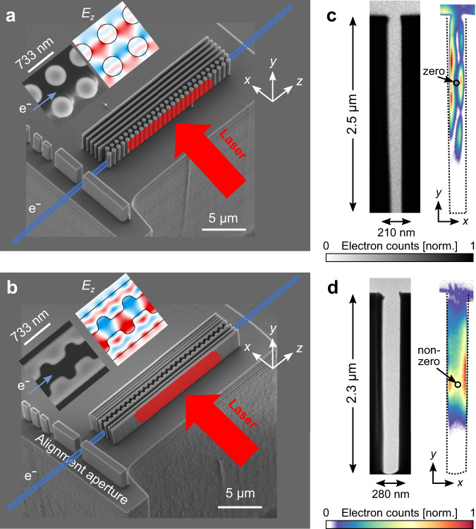
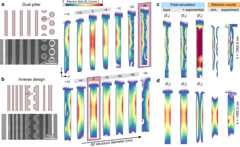
Controlling optical fields on the subwavelength scale is at the core of nanophotonics. Laser-driven nanophotonic particle accelerators promise a compact alternative to conventional radiofrequency-based accelerators. Efficient electron acceleration in nanophotonic devices critically depends on achieving nanometer control of the internal optical nearfield. However, these nearfields have so far been inaccessible due to the complexity of the devices and their geometrical constraints, hampering the design of future nanophotonic accelerators. Here we image the field distribution inside a nanophotonic accelerator, for which we developed a technique for frequency-tunable deep-subwavelength resolution of nearfields based on photon-induced nearfield electron-microscopy. Our experiments, complemented by 3D simulations, unveil surprising deviations in two leading nanophotonic accelerator designs, showing complex field distributions related to intricate 3D features in the device and its fabrication tolerances. We envision an extension of our method for full 3D field tomography, which is key for the future design of highly efficient nanophotonic devices.


Conflict of interest statement

The authors declare no competing interests.

Figures

Fig. 1
Fig. 1. Imaging the field distribution inside dielectric laser acceleration (DLA) structures.
a An illustration of the transmission electron microscope experimental setup. A LaB6 electron source operates in thermionic mode; a set of magnetic lenses and apertures are used to condition the electron beam such that it enters the DLA parallel to the channel at the required spot size; a 1064 nm CW laser modulates the energy of the electrons passing through the 20 μm long DLA structure; the electrons continue to a spectrometer, where they are energy-filtered such that only electrons that gained energy are imaged. b, c 3D model of the two structures used in this work: a dual-pillar structure with a distributed Bragg reflector and an inverse-designed resonant structure, respectively. A representative field distribution is overlaid at the end of the channel. d Measured (black crosses) and simulated (blue line) electron energy loss spectra (EELS) at representative locations inside the channel of the inverse-designed structure. These energy spectra measurements are obtained with an electron beam spot size of ~70 nm, which is smaller than the channel widths of 210 and 280 nm in the two DLA structures. In contrast, the electron beam used to image the field distributions (insets of b and c) has a spot of ~3μm, sufficiently large to cover the entire electron channel. The gray region in the spectra was filtered out to obtain the images of the acceleration field profile. Since the driving field amplitude is about three orders of magnitude smaller than that of fs pulses, the peak energy gain inside the CW-driven DLA structures reaches 5 eV (g=1.2), which in the classical picture corresponds to an acceleration gradient of about 0.2 MeV/m along the effective interaction length of 15 µm, given by the laser spot size. Compared to the much higher acceleration gradients of typically used fs laser pulses, the weak CW light field offers three advantages: (1) The weak field guarantees that the electron energy spectrum is not saturated, i.e., the zero-loss peak in the EELS is not fully depleted, which means that the electron counts monotonically increase with electric field strength. Stronger fields also cause transverse motion of the electron, which reduces the spatial resolution. (2) The CW operation enables working with continuous electron beams, which have much higher flux and better electron beam quality, thus providing better image quality. (3) The narrow bandwidth of CW light enables scanning over the wavelength with sub-nm resolution, which is much narrower than the bandwidth of fs pulses, and reveals the fine spectral response of the DLA. e Calculated transformation curve between measured EFTEM counts and the acceleration coefficient g, which is proportional to Ez(x,y). The values of g obtained from the fits in d are marked with colored dots.
Fig. 2
Fig. 2. Scanning electron microscopy images of the dielectric laser acceleration (DLA) structures.
The electrons (blue) enter the structures via an alignment aperture and are accelerated in the structure by the electric field of a 1064 nm CW laser impinging on the structure perpendicular to the electron flow. The laser illumination area is marked as a red surface showing that the spot diameter of 15 μm (1/e2) is smaller than the structure length of 20 μm. a, b The dual-pillar structure with Bragg mirror and the resonance-enhanced inverse-designed structure, respectively. A zoom-in view into the structure and the corresponding accelerating electric field distribution Ez(x,z) are shown as insets for both structures. The periodicity of 733 nm provides phase matching between the electrons and the electric field along the z-direction. Note that Ez has a substantial non-vanishing value at the center of the channel, where electrons are guided. c, d Typical TEM images of the two DLA channels were taken with a broad 3 μm spot-size electron beam, without (left, black-white color scale) and with (right, rainbow color scale) electron energy filtering. The unfiltered image shows the uniformly illuminated electron channel, revealing a slightly conical shape of the pillars with a slightly narrower channel at the bottom. The filtered image shows the measured PINEM field distribution, which extends above the structure’s top and vanishes far above the channel’s bottom in both cases. In addition, the field measured in the dual-pillar (c) structure has a null at the center, which is different from its design (as discussed below).
Fig. 3
Fig. 3. Measured spectral response of the field distribution inside the DLA channel.
Our method for deep-subwavelength spatial imaging with sub-nm spectral resolution is applied to (a) the dual-pillar structure and (b) the inverse-designed structure. We observe a substantial change for the inverse-designed structure and hardly any change for the dual-pillar structure. c, d Measured field cross section (blue/purple dots) along the red marking lines in a and b. The black dashed lines (which can hardly be distinguished from the blue/purple dots since they almost perfectly overlap) are fits of the expected cosh/sinh field profile within the channel. They were multiplied by an exponential decay at the edges of the channel, where electrons lose energy due to inelastic scattering off the structure. A Gaussian convolution imitates the blurring effect mainly due to the imaging point spread function. The dual-pillar structure has a large sinh component in the fit, which corresponds to an anti-symmetric (odd) structural mode with zero field at the center. In contrast, the inverse-designed structure has a substantial cosh component in the fit, with large non-vanishing energy at the channel center corresponding to a low-order symmetric (even) mode.
Fig. 4
Fig. 4. Sensitivity of the DLA nearfield to changes in structure geometry.
The accelerating field distribution Ez(x,y) is investigated by 3D simulations as a function of deviations δD from the nominal size D, marked in the SEM images on the left. a, b Dual-pillar and inverse-designed structures, showing field simulations for a scan over δD=+14 to 40nm and δD=+10 to 44nm, respectively. The best fit results are obtained for δD=48nm and δD=0 for the dual-pillar and inverse-designed structures, respectively. Near the design target (δD=0), the symmetric mode is dominant for both structures, as designed. For small changes δD, the field maxima move from side to side with increasing contribution from the anti-symmetric mode. Close to the best fit result of the dual-pillar structure (δD=40nm, marked by red rectangle), its anti-symmetric mode is highly robust against changes in δD. These simulation results match the experimental findings of Fig. 3, where the symmetric mode of the inverse-designed structure moves from side to side, whereas the anti-symmetric mode of the dual-pillar structure does not change much with wavelength. c, d Side-by-side comparison of measured and best-fit simulated EFTEM images. For the conversion from electric field to electron counts, we normalized by assuming that the maximum coupling constant g inside the channel reaches 1.8, which is close to the experimentally found value from Fig. 1e. Looking at the deflecting field Ex(x,y) reveals that a symmetric mode in Ez is associated with an anti-symmetric mode in Ex and vice versa.
Fig. 5
Fig. 5. Proposal for 3D tomography of the field distribution inside a DLA structure.
To gain information about how the nearfield behaves along the length of the structure, we suggest illuminating sequentially individual sub-sections, one at a time, to reconstruct the full 3D field. This can be either achieved by (a) including an aperture on the chip design. For each position, a dedicated test structure would be added to the chip. b Alternatively, a lens can be used to focus the laser to a small spot of a few µm. Scanning the beam along the structure would then provide full 3D field information. A deconvolution algorithm can further increase the spatial resolution along the channel. Simulations of the two approaches are shown in Supplementary Fig. S5.

References

    1. Hamm, R. W. & Hamm, M. E. Industrial accelerators and their applications (World Scientific, 2012).
    1. Samy, H. RF linear accelerators for medical and industrial applications, 1st edn (Artech House, 2012).
    1. Apollinari, G. et al. High-Luminosity Large Hadron Collider (HL-LHC) (CERN, 2017).
    1. England RJ, et al. Dielectric laser accelerators. Rev. Mod. Phys. 2014;86:1337–1389. doi: 10.1103/RevModPhys.86.1337. - DOI
    1. Ruimy R, Gorlach A, Mechel C, Rivera N, Kaminer I. Toward atomic-resolution quantum measurements with coherently shaped free electrons. Phys. Rev. Lett. 2021;126:233403. doi: 10.1103/PhysRevLett.126.233403. - DOI - PubMed