Review
. 2023 Jun 7;13(12):1818.
doi: 10.3390/nano13121818.

Laser Interference Lithography-A Method for the Fabrication of Controlled Periodic Structures

Affiliations
Review

Laser Interference Lithography-A Method for the Fabrication of Controlled Periodic Structures

Ri Liu et al. Nanomaterials (Basel). .

Abstract

A microstructure determines macro functionality. A controlled periodic structure gives the surface specific functions such as controlled structural color, wettability, anti-icing/frosting, friction reduction, and hardness enhancement. Currently, there are a variety of controllable periodic structures that can be produced. Laser interference lithography (LIL) is a technique that allows for the simple, flexible, and rapid fabrication of high-resolution periodic structures over large areas without the use of masks. Different interference conditions can produce a wide range of light fields. When an LIL system is used to expose the substrate, a variety of periodic textured structures, such as periodic nanoparticles, dot arrays, hole arrays, and stripes, can be produced. The LIL technique can be used not only on flat substrates, but also on curved or partially curved substrates, taking advantage of the large depth of focus. This paper reviews the principles of LIL and discusses how the parameters, such as spatial angle, angle of incidence, wavelength, and polarization state, affect the interference light field. Applications of LIL for functional surface fabrication, such as anti-reflection, controlled structural color, surface-enhanced Raman scattering (SERS), friction reduction, superhydrophobicity, and biocellular modulation, are also presented. Finally, we present some of the challenges and problems in LIL and its applications.

Keywords: laser interference lithography; laser materials processing; micro/nanostructuring; periodic structure; surface functionalization.


Conflict of interest statement

The authors declare no conflict of interest.

Figures

Figure 1
Figure 1
MATLAB simulations of interfering light fields: (A,B) stripe arrays obtained from double-beam LIL at different incidence angles. (CE) Dot/hole arrays obtained from triple-beam LIL at different azimuthal angles. (F,G) Dot/hole arrays obtained from quadruple-beam LIL at different incidence angles. (HJ) Dot/hole arrays produced by quadruple-beam LIL at different azimuthal angles. Reproduced with permission/adapted from [16].
Figure 2
Figure 2
AFM images of a single-pulse double-beam LIL: (ac) for exposure energies of 560 mJ·cm−2, 630 mJ·cm−2, and 700 mJ·cm−2; (df) are views of the cross-sectional wheelhouse for (a), (b), and (c), respectively. Reproduced with permission/adapted from [25].
Figure 3
Figure 3
(a) Schematic illustration of the interference geometry. (b) Simulation results of the interference patterns using the geometry in (a) with the polarization direction of the input laser beam changed from α = 0 to 90 degrees with respect to the vertical direction. (c) Experimental results of the produced photoresist grating structures. Cross-section demonstration of the fabricated structures with α = 40°, where the sample was cut along the dashed pink line in (b). Reproduced with permission/adapted from [29].
Figure 4
Figure 4
MATLAB simulations of LIL for three different polarization modes: The TE-TE-TE-TE mode includes figure (a) with the same angle of incidence and figure (c) with a misaligned angle of incidence. The TE-TE-TE-TM mode includes figure (e) with the same angle of incidence and figure (g) with a mis-aligned angle of incidence. The TE-TE-TM-TM pattern includes figure (i) with the same angle of incidence and figure (k) with a misaligned angle of incidence. (b,d,f,h,j,l) are the intensity profiles along the double-arrow lines in (a,c,e,g,i,k), respectively. Reproduced with permission/adapted from [26].
Figure 5
Figure 5
Schematic diagram of the structure with reduced reflection of the incident light. (a) Propagation of incident light through a single layer film on a substrate (ns > n). (b) Multiple internal reflections of incident light in a microstructure array. (c) Interaction of incident light with the subwavelength-size nanoarray. (d) Schematic illustration of the refractive index change corresponding to (c). Reproduced with permission/adapted from [39].
Figure 6
Figure 6
(af) Cross-sectional and top-view SEM images of the samples. (gi) SEM images of samples (S1, S2, and S3) placed at 45°, 30°, and 45°, respectively. Scale bar: 1 μm. (j) Photograph of the DI water, HCl, and NaOH droplets on sample S3 (scale bar: 1 cm). (k) SEM image corresponding to sample S3 (scale bar: 10 μm). (l) The simulated (red curve) and experimental (black curve) reflectance spectra of the hierarchical moth-eye structure. The inset is the reflectance spectrum in the mid-infrared range. Reproduced with permission/adapted from [45].
Figure 7
Figure 7
(a) Photograph of the stainless steel surface treated with different numbers of pulses (from 1 to 5) and laser fluences (from 0.7 to 11.4 J/cm2); (b) confocal image of LIL holographic pixels on the steel surface with a diameter of approximately 50 µm; (c) typical hole-like pattern with a spatial period of 1.8 µm and a structure depth of 0.3 µm (the used laser fluence was 1.9 J/cm2 and three pulses were applied). Reproduced with permission/adapted from [47].
Figure 8
Figure 8
(a) An experimental setup to realize the helical photonic crystals with a submicron scale spatial and axial periodicity; 50:50 ultraviolet beam splitter for 405 nm; the microscopic objective of 10×; SEM images of the fabricated submicron periodic helical photonic crystal structure on positive photoresist (AZ 1518). (b) Cross-sectional 45° tilt view presenting the realization of 3D periodic structures over a large area; the inset shows another sample with different exposures in the isometric view obtained through tilt and rotation of the sample stage. (c) Cross-sectional view of a purposely broken sample with less exposure time. (The inset shows a magnified view with chirality properly marked). (d) A 45° tilt view of a single-layer helical structure over a single pitch in negative photoresist (marked by dotted circle). Reproduced with permission/adapted from [41].
Figure 9
Figure 9
(a,b) SEM images of periodic variable-sized platinum nanoparticles (PtNPs) fabricated by double-beam LIL and (c) the distribution bar of different sizes of platinum nanoparticles (PtNPs) within an area of T × T along the period, where T is the period. Reproduced with permission/adapted from [33].
Figure 10
Figure 10
(a) Ordered Ag patterns obtained by SELIL. (b) Ag nanocavities at high magnification. (c) Corresponding hybrid SiNW and SiNH arrays after MACE for 30 min, and (d) SiNWs at high magnification. (eg) SEM cross-sectional images of hybrid SiNW and SiNH arrays etched for (e) 5, (f) 10, and (g) 30 min; and (h) the relationship between the etching depth and etching time. Reproduced with permission/adapted from [100].
Figure 11
Figure 11
Experimental setup and formation schematic of the laser interference-induced forward transfer PI micro-stripes. (a) Schematic diagram of the double-beam LIIFT configuration. (b) The fabrication schematic of micro-stripes in LIIFT, and the micro-stripes eject from the PI-donor film to the receiving substrate. (c) The transferred micro-stripes from the donor-film 1.2 µm with the laser fluence 39 mJ·cm−2 and pulse number 50. Reproduced with permission/adapted from [105].
Figure 12
Figure 12
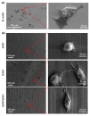
(a) SEM images of A549 cells cultured on the silicon wafer for 24 h. The image on the right side shows the details of cells in the red box with a high magnification. (b) SEM images of A549 cells cultured on the silicon nanopillar (SiNP) arrays, SiNH, and SiNP/SiNH arrays for 24 h. The images on the right side show the details of cells in the red boxes with a high magnification. Reproduced with permission/adapted from [114].
Figure 13
Figure 13
(a) Illustration of the direct laser interference patterning process for double-beam LIL and (b) the experimental setup of the LIL system with a ps laser source. Reproduced with permission/adapted from [18]. (c,d) SEM images of samples patterned with hierarchical microstructures, via LIL and direct laser writing techniques. Reproduced with permission/adapted from [151].
Figure 14
Figure 14
(a) Images of the contact angle and the shape of water droplets on a natural taro leaf surface; SEM images of the taro leaf surface structures. (b) Images of the contact angle and the shape of water droplets on the processed HC surface; SEM images of the processed HC surfaces. The microstructures consisted of the micropillar array with the period of 10 μm; The nanostructure array covered the entire microstructure surface, and the nanostructure was composed of TiO2 nanoscale grasses with the diameter of −40 nm and height of −1.5 μm. (c) The photos of the untreated surfaces (US)-, MPA-, NG-, and HC- surfaces (from the top to bottom). The reference droplets (4 μL tap water) were placed on the four surfaces at −10 °C. All of the droplets were initially transparent. Following the DT of 18 s, the droplet became opaque on the US surface; after 87 s, another droplet was opaque on the MPA surface. Following 1053 s of DT, the droplets also became opaque on the NG surface. Prior to the time of 3709 s, the droplets on the HC surface were still transparent. For the next 23 s, the droplets gradually froze and the transmittance decreased. At 3732 s, the droplets became opaque. Reproduced with permission/adapted from [155].
Figure 15
Figure 15
(a) SEM image of the microstructure fabricated by triple-beam LIL; (b) close-up image of the structured surface; (c) SEM image of Vickers’ indentation with the applied load of 200 g for 10 s; (d) SEM image of the original material with Vickers’ indentation. (e) Schematic of the lubrication model reducing friction by the formation of dimples. Reproduced with permission/adapted from [130].

References

    1. Bhushan B., Jung Y.C. Natural and biomimetic artificial surfaces for superhydrophobicity, self-cleaning, low adhesion, and drag reduction. Prog. Mater. Sci. 2011;56:1–108. doi: 10.1016/j.pmatsci.2010.04.003. - DOI
    1. Xia F., Jiang L. Bio-Inspired, Smart, Multiscale Interfacial Materials. Adv. Mater. 2008;20:2842–2858. doi: 10.1002/adma.200800836. - DOI
    1. Malshe A.P., Bapat S., Rajurkar K.P., Haitjema H. Bio-inspired textures for functional applications. CIRP Ann. 2018;67:627–650. doi: 10.1016/j.cirp.2018.05.001. - DOI
    1. Si Y., Dong Z., Jiang L. Bioinspired Designs of Superhydrophobic and Superhydrophilic Materials. ACS Cent. Sci. 2018;4:1102–1112. doi: 10.1021/acscentsci.8b00504. - DOI - PMC - PubMed
    1. Tan Y., Hu B., Song J., Chu Z., Wu W. Bioinspired Multiscale Wrinkling Patterns on Curved Substrates: An Overview. Nano-Micro Lett. 2020;12:1–42. doi: 10.1007/s40820-020-00436-y. - DOI - PMC - PubMed

LinkOut - more resources