Review
. 2023 Jul 14;12(1):175.
doi: 10.1038/s41377-023-01173-8.

Recent progress in quantum photonic chips for quantum communication and internet

Affiliations
Review

Recent progress in quantum photonic chips for quantum communication and internet

Wei Luo et al. Light Sci Appl. .

Abstract

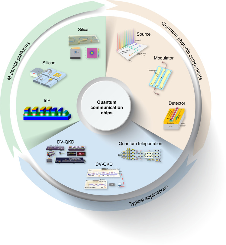
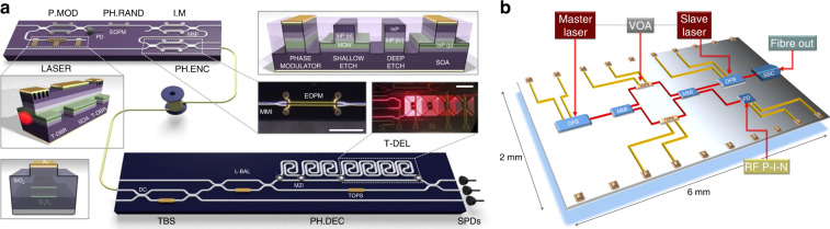
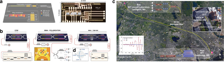
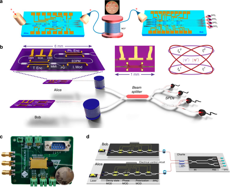
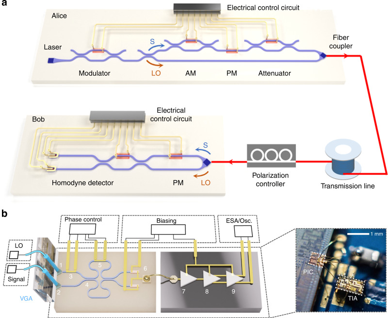
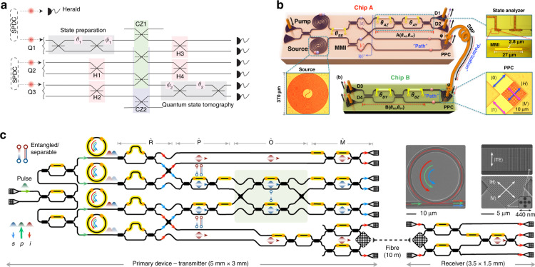
Recent years have witnessed significant progress in quantum communication and quantum internet with the emerging quantum photonic chips, whose characteristics of scalability, stability, and low cost, flourish and open up new possibilities in miniaturized footprints. Here, we provide an overview of the advances in quantum photonic chips for quantum communication, beginning with a summary of the prevalent photonic integrated fabrication platforms and key components for integrated quantum communication systems. We then discuss a range of quantum communication applications, such as quantum key distribution and quantum teleportation. Finally, the review culminates with a perspective on challenges towards high-performance chip-based quantum communication, as well as a glimpse into future opportunities for integrated quantum networks.


Conflict of interest statement

The authors declare no competing interests.

Figures

Fig. 1
Fig. 1. Overview of quantum photonic chips for quantum communication.
The research scope covers photonic materials platforms for large-scale integration, quantum photonic components such as quantum light sources, high-speed modulators, and highly efficient photodetectors, as well as typical applications in QKD, and quantum teleportation. Panels reproduced with permission from: ref. , Springer Nature Ltd; ref. , under a Creative Commons licence (https://creativecommons.org/licenses/by/4.0/); ref. , AIP Publishing LLC; ref. , under a Creative Commons licence (https://creativecommons.org/licenses/by/4.0/); ref. , Springer Nature Ltd; ref. , under a Creative Commons licence (http://creativecommons.org/licenses/by-nc-nd/3.0/); ref. , under a Creative Commons licence (https://creativecommons.org/licenses/by/4.0/); ref. , Springer Nature Ltd; ref. , Springer Nature Ltd
Fig. 2
Fig. 2. Timeline of advances in quantum photonic chips for quantum communication.
The key milestones include the first demonstrations of the on-chip quantum interferometer for quantum cryptography, quantum teleportation on a photonic chip, chip-based DV-QKD, CV-QKD, and MDI-QKD,,, and chip-to-chip quantum teleportation. Panels reproduced with permission from: ref. , Institution of Electrical Engineers; ref. , Springer Nature Ltd; ref. , under a Creative Commons licence (https://creativecommons.org/licenses/by/4.0/); ref. , Springer Nature Ltd; ref. , Springer Nature Ltd
Fig. 3
Fig. 3. On-chip QD photon sources.
a An illustration of a single InAs/GaAs self-assembled QD embedded in a 2.5-μm-diameter micropillar cavity. b Schematic of an InGaAs QD coupled to a micropillar that is connected to a surrounding circular frame by four one-dimensional wires. c A single QD embedded in a photonic crystal waveguide. A large portion of emitted single photons is channeled with near-unity probability into the waveguide mode. d An illustration of a circular Bragg resonator on a highly efficient broadband reflector with a single GaAs QD emitting entangled photon pairs. Panels reproduced with permission from: a ref. , APS; b ref. , Springer Nature Ltd; c ref. , APS; d ref. , Springer Nature Ltd
Fig. 4
Fig. 4. Different types of chip-based parametric photon sources.
a Array of spontaneous four-wave mixing (SFWM) heralded single-photon sources (HSPSs). A series of straight waveguides are fabricated via UV-laser writing in a germanium-doped silica-on-silicon photonic chip, each of which constitutes its own HSPS. b A nanophotonic visible–telecom SFWM photon-pair source using high-quality factor silicon nitride resonators to generate narrow-band photon pairs with unprecedented purity and brightness. c A spontaneous parametric down-conversion (SPDC) entangled photon source based on a LN photonic chip with a periodically poled section. Panels reproduced with permission from: a ref. , under a Creative Commons licence (https://creativecommons.org/licenses/by/4.0/); b ref. , Springer Nature Ltd; c ref. , APS
Fig. 5
Fig. 5. Typical integrated components on quantum photonic chips.
a Schematics of a polarization splitter/rotator and the evolution of its mode profile. b Optical micrograph and perspective view of a thermo-optic phase shifter in silicon. c Schematic of a high-bandwidth electro-optic modulator, where an unpatterned LN thin film is bonded to a Mach-Zehnder interferometer fabricated in Si. d Schematic of a directional coupler with a thin layer of Ge2Sb2Te5 (GST). e Schematic of a 4 × 4 multi-mode interferometer. f Schematic of a hybrid quantum photonic circuit integrated with an on-chip tunable ring resonator filter. g Schematic of a silicon photonic waveguide spiral delay line. (h) A six-mode universal linear-optic device that was realized in a fully re-programmable silica chip. Panels reproduced with permission from: a ref. , The Optical Society; b ref. , The Optical Society; c ref. , The Optical Society; d ref. , American Chemical Society; e ref. , under a Creative Commons licence (http://creativecommons.org/licenses/by-nc-nd/3.0/); f ref. , under a Creative Commons licence (https://creativecommons.org/licenses/by/4.0/); g ref. , Chinese Laser Press; h ref. , AAAS
Fig. 6
Fig. 6. Overview of on-chip single-photon detector (SPD) and homodyne detector.
a Angled scanning electron microscope image of a waveguide-coupled Ge-on-Si lateral single-photon avalanche photodiode with oxide cladding removed. b A NbN nanowire traveling wave SNSPD atop a silicon waveguide with detection efficiency up to 91%. c A waveguide photon-number resolving (PNR) SNSPD consisting of four wires in series with a resistance (Rp) in parallel to each wire. d Membrane transfer of a hairpin-shaped NbN SNSPD onto a photonic waveguide for on-chip detection of non-classical light. e A silicon-based homodyne detector with a thermo-optical phase shifter, two Mach–Zehnder modulators and two photodiodes, interfaced to a customized transimpedance amplifier by wire bonding. Panels reproduced with permission from: a ref. , The Optical Society; b ref. , under a Creative Commons licence (http://creativecommons.org/licenses/by-nc-nd/3.0/); c ref. , AIP Publishing LLC; d ref. , under a Creative Commons licence (https://creativecommons.org/licenses/by/4.0/); e ref. , The Optical Society
Fig. 7
Fig. 7. Instances of chip packaging and integration.
a Schematic of a bilayer LN inverse taper coupled with a lensed optical fiber. b Schematic of a Si3N4-on-SOI dual-level grating coupler interfaced with a single-mode fiber. c Photograph of a quantum photonic processor packaged with PCBs, fiber arrays and thermoelectric cooler. d Photograph of an assembled multi-chip module that provides connectivity between one photonic integrated circuit (IC) and four electronic ICs via silicon interposer. Panels reproduced with permission from: a ref. , The Optical Society; b ref. , The Optical Society; c ref. , under a Creative Commons licence (https://creativecommons.org/licenses/by/4.0/); d ref. , under a Creative Commons licence (https://creativecommons.org/licenses/by/4.0/)
Fig. 8
Fig. 8. Integrated quantum random number generators (QRNGs).
a A QRNG by measuring phase fluctuations from a laser diode with an SOI chip. b A hybrid integrated QRNG with InGaAs photodiodes packaged on a SOI chip. Panels reproduced with permission from: a ref. , Creative Commons licence (https://creativecommons.org/licenses/by/4.0/); b ref. , AIP Publishing LLC
Fig. 9
Fig. 9. Chip-based QKD systems with hybrid materials platform.
a A chip-to-chip system with a 2 × 6 mm2 integrated indium phosphide (InP) transmitter and a 2 × 32 mm2 silicon oxynitride (SiOxNy) photonic receiver circuit for GHz clock rate, reconfigurable, multi-protocol QKD. b A modulator-free QKD transmitter chip consisting of two cascaded high-bandwidth distributed feedback lasers and one variable optical attenuator. Panels reproduced with permission from: a ref. , under a Creative Commons licence (https://creativecommons.org/licenses/by/4.0/); b ref. , under a Creative Commons licence (https://creativecommons.org/licenses/by/4.0/)
Fig. 10
Fig. 10. Silicon photonic chips for multiple QKD protocols.
a A Si transmitter for polarization-encoded QKD, consisting of a microring pulse generator, a microring intensity modulator, four variable optical attenuators, and a polarization controller. b Integrated silicon photonic transmitters to perform multiple QKD protocols, including coherent-one-way, polarization encoded BB84 and time-bin encoded BB84. c Field test of intercity QKD over a 43-km dark fiber link using a silicon photonic polarization encoder. Panels reproduced with permission from: a ref. , The Optical Society; b ref. 155, under a Creative Commons licence (https://creativecommons.org/licenses/by/4.0/); c ref. , under a Creative Commons licence (https://creativecommons.org/licenses/by/4.0/)
Fig. 11
Fig. 11. Different chip-based quantum communication systems for advanced QKD protocols.
a Silicon-photonic-integrated circuit for noise-tolerant high-dimensional QKD. b InP transmitter chips used to generate the time-bin encoded BB84 weak coherent states for MDI-QKD. c A packaged silicon photonic MDI-QKD transmitter chip soldered to a compact control board. d A silicon photonic chip-based MDI-QKD system comprising two transmitter chips and one server chip interfaced with off-chip SPDs. Panels reproduced with permission from: a ref. , under a Creative Commons licence (https://creativecommons.org/licenses/by/4.0/); b ref. , under a Creative Commons licence (https://creativecommons.org/licenses/by/4.0/); c ref. , under a Creative Commons licence (https://creativecommons.org/licenses/by/4.0/); d ref. , APS
Fig. 12
Fig. 12. Integrated circuits for continuous variable (CV) QKD and high-speed homodyne detection.
a An integrated silicon photonic chip platform for CV-QKD, consisting of a transmitter for signal modulation and multiplexing and a receiver for signal demultiplexing and homodyne detection. b A silicon photonic homodyne detector interfaced with integrated electronics for 9-GHz measurement of squeezed light. Panels reproduced with permission from: a ref. , Springer Nature Ltd; b ref. , Springer Nature Ltd
Fig. 13
Fig. 13. Chip-based quantum teleportation and entanglement distribution systems.
a Scheme of an on-chip quantum teleportation experiment in a silica-on-silicon integrated chip. b Silicon photonic circuit diagram for a chip-to-chip entanglement distribution experiment. c Photonic circuit diagram for a chip-to-chip quantum teleportation experiment. Panels reproduced with permission from: a ref. , Springer Nature Ltd; b ref. , The Optical Society; c ref. , Springer Nature Ltd

References

    1. Bennett CH, Brassard G. Proc. International Conference on Computers, Systems & Signal Processing. Bangalore: IEEE; 1984. Quantum cryptography: public key distribution and coin tossing; pp. 175–179.
    1. Bennett CH, et al. Experimental quantum cryptography. J. Cryptol. 1992;5:3–28. doi: 10.1007/BF00191318. - DOI
    1. Shor PW, Preskill J. Simple proof of security of the BB84 quantum key distribution protocol. Phys. Rev. Lett. 2000;85:441–444. doi: 10.1103/PhysRevLett.85.441. - DOI - PubMed
    1. Gisin N, et al. Quantum cryptography. Rev. Mod. Phys. 2002;74:145–195. doi: 10.1103/RevModPhys.74.145. - DOI
    1. Xu FH, et al. Secure quantum key distribution with realistic devices. Rev. Mod. Phys. 2020;92:025002. doi: 10.1103/RevModPhys.92.025002. - DOI