Review
. 2023 Jul 5;13(13):2011.
doi: 10.3390/nano13132011.

Advancing Thermoelectric Materials: A Comprehensive Review Exploring the Significance of One-Dimensional Nano Structuring

Affiliations
Review

Advancing Thermoelectric Materials: A Comprehensive Review Exploring the Significance of One-Dimensional Nano Structuring

Mustafa Majid Rashak Al-Fartoos et al. Nanomaterials (Basel). .

Abstract

Amidst the global challenges posed by pollution, escalating energy expenses, and the imminent threat of global warming, the pursuit of sustainable energy solutions has become increasingly imperative. Thermoelectricity, a promising form of green energy, can harness waste heat and directly convert it into electricity. This technology has captivated attention for centuries due to its environmentally friendly characteristics, mechanical stability, versatility in size and substrate, and absence of moving components. Its applications span diverse domains, encompassing heat recovery, cooling, sensing, and operating at low and high temperatures. However, developing thermoelectric materials with high-performance efficiency faces obstacles such as high cost, toxicity, and reliance on rare-earth elements. To address these challenges, this comprehensive review encompasses pivotal aspects of thermoelectricity, including its historical context, fundamental operating principles, cutting-edge materials, and innovative strategies. In particular, the potential of one-dimensional nanostructuring is explored as a promising avenue for advancing thermoelectric technology. The concept of one-dimensional nanostructuring is extensively examined, encompassing various configurations and their impact on the thermoelectric properties of materials. The profound influence of one-dimensional nanostructuring on thermoelectric parameters is also thoroughly discussed. The review also provides a comprehensive overview of large-scale synthesis methods for one-dimensional thermoelectric materials, delving into the measurement of thermoelectric properties specific to such materials. Finally, the review concludes by outlining prospects and identifying potential directions for further advancements in the field.

Keywords: electrical conductivity; figure-of-merit; materials; nanostructuring; one dimensional; seebeck coefficient; thermal conductivity; thermoelectric.


Conflict of interest statement

The authors declare no conflict of interest.

Figures

Figure 6
Figure 6
(a) Atomic structures of a bulk unit cell of Bi2Te3 “Reproduced with permission from [51], WILEY-VCH, 2019”. (b) Typical PbTe cell displayed with simple cubic structure “Reproduced with permission from [61], American Physical Society, 2012”. (c) The unit cell of α-SnSe crystal structure “Reproduced with permission from [62], Elsevier, 2018”. (d) Crystal structure of the SiGe “Reproduced with permission from [63], Woodhead, 2011”.
Figure 7
Figure 7
(a) Crystal structure of CoSb3, where small pink is Co, small yellow is Sb atoms, and the large blue sphere is filler “Reproduced with permission from [131], American Physical Society, 2011”. (b) Temperature-dependent ZT value of single, double, and multiple filled skutterudites “Reproduced with permission from [87], American Chemical Society, 2011”. (c) The crystal structure of Yb14MnSb11 along the c axis. Yb, Mn, and Sb atoms are indicated by green, orange, and blue spheres, respectively. “Reproduced with permission from [93], American Chemical Society, 2015”. (d) Unit cell of the clathrate type-I Eu8Ga16Ge30 “Reproduced with permission from [100], American Physical Society, 2013”. (e) Crystal structure of NaxCoO2 “Reproduced with permission from [132], American Physical Society 2006”. (f) The crystal structure of different Cu2−xS “Reproduced with permission from [124], Elsevier, 2021”.
Figure 8
Figure 8
(a) Crystal structure of the Half-Heusler (MgAgAs type) phase. (b) The huge number of elements in the Periodic table of the elements that is possible to form Heusler compounds “Reproduced with permission from [164], Elsevier, 2019”. (c) TE carbon nano tube structure “Reproduced with permission from [144], MDPI, 2019”. (d) Schematic illustration of designed ternary TE composites paper “Reproduced with permission from [151], WILEY-VCH, 2016”.
Figure 10
Figure 10
(a) The effect of the porosity on the phonon and electron path. (b) The effect of the porosity on the thermal conductivity Bi2Te2.56Se0.44 “Reproduced with permission from [187], WILEY-VCH, 2017”. (c) This simplified Figure depicts the mechanism of phonon scattering and the flow of hot and cold electrons through a TE material, “Reproduced with permission from [219], WILEY-VCH, 2010”. (d) Temperature dependence of ZT of PdS. (e) Pressure dependent ZT of PdS around room temperature “Reproduced with permission from [212], Elsevier, 2018”. (f) Structure of superlattice “Reproduced with permission from [215], Royal Society Of Chemistry, 2012”.
Figure 11
Figure 11
(a) The phase transition between the rhombohedral and cubic phase in Sb-doped GeTe. (b) The schematic diagram illustrates the thermal conductivity of PbTe NWs and PbTe0.5Se0.5 bulks “Reproduced with permission from [224], Elsevier, 2020”. (c) The density of states (DOS) of bulk (3D), 2D, and 1D materials as a function of energy and, by lowering the dimensions, the (DOS) is enhanced. “Reproduced with permission from [234], WILEY-VCH, 2020”.
Figure 12
Figure 12
(a) effect the quantum wire diameter of Si on the band gap “Reproduced with permission from [237] American Physical Society, 2007” (b) TEM image of 9.5 nm diameter QWs “Reproduced with permission from [244], American Chemical Society, 2021”.
Figure 13
Figure 13
(a) SEM image of Bi nanowires “Reproduced with permission from [262], American Chemical Society, 2014”. (b) The pearl-necklace-shaped PbTe NWs “Reproduced with permission from [255], American Chemical Society, 2008”. (c) Si NWs array. (d) Si nanowire and its roughness are clearly seen at the surface of the wire “Reproduced with permission from [257], American Chemical Society, 2020”. (e) ZnO NWs (f) ZnO NWs array “Reproduced with permission from [263], American Chemical Society, 2006”.
Figure 14
Figure 14
(a) The procedure of coating glass fibre with PbTe. (b) PbTe nanocrystal-coated glass fibres “Reproduced with permission from [266], American Chemical Society, 2012” (c) SEM image of the fibre connected by electrodes on substrate for thermal conductivity measurements, “Reproduced with permission from [267], American Chemical Society, 2013”. (d) Schematic of thermal drawing of SnSe fibre and post-draw laser recrystallization process (e) Single SnSe fibre with good flexibility (f) Photograph of SnSe fibres that are tens of metres long “Reproduced with permission from [270], WILEY-VCH, 2020”.
Figure 15
Figure 15
(a) The Bi2Te3/Te NWs array (b) Close up on Bi2Te3(II)/Te(I) segments (c) HRTEM image and SAED patterns of each segment “Reproduced with permission from [274], American Chemical Society, 2007”.
Figure 16
Figure 16
(a) (Bi2Te3-ySey) nanotubes. (b) (Bi2−xSbxTe3) nanotubes “Reproduced with permission from [284], American Chemical Society, 2008”. (c) TEM images of individual CNTs coated with a PANI layer that indicates by white arrows. (d) CNT bundles coated with a PANI layer that indicates by white arrows “Reproduced with permission from [290], WILEY-VCH, 2010”. (e) PbTe nanotubes. (f) PbTe single nanotube “Reproduced with permission from [292], Elsevier, 2018”.
Figure 17
Figure 17
(a) Schematic steps for electrochemical deposition method “Reproduced with permission from [317], Elsevier, 2021”. (b) Schematic illustration of hydrothermal mechanism “Reproduced with permission from [329], Society of Chemistry, 2015”. (c) Schematic illustration of VLS mechanism of SiNWs growth “Reproduced with permission from [336], Hindawi, 2013”. (d) Electroless etching mechanism “Reproduced with permission from [336], Hindawi, 2013”. (e) The SEM images of the cross section of the silicon etched in the AgNO3/HF solution “Reproduced with permission from [338], Elsevier, 2011”.
Figure 18
Figure 18
(a) Schematic illustrating the four-probes electrical conductivity measuring methods. (b) Schematic illustrating van der Pauw’s electrical conductivity measuring methods. (c) Schematic illustrating the Seebeck measuring device of the vertical TE thin film generator “Reproduced with permission from [343], Elsevier, 2019”. (d) Schematic illustrating in-plane Seebeck measuring device for TE thin film generator “Reproduced with permission from [347], MDPI, 2021”. (e) Schematic illustrating of the 3ω method for measuring thermal conductivity for thin films “Reproduced with permission from [344], AIP, 2018”. (f) Image of microchip device used to measure of the TE performance of individual NWs accurately.
Figure 1
Figure 1
Comparison of publications on 1D TE and TE and application distribution across disciplines for 1D TE materials [15].
Figure 2
Figure 2
The key achievements in the evolution of the TE sector.
Figure 3
Figure 3
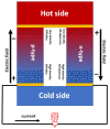
Schematic illustrating the working principle of TE materials.
Figure 4
Figure 4
The theoretical density of states (DOS) with (a) Large slope (b) Slight slope “Reproduced with permission from [36], WILEY-VCH, 2009”. (c) The effect of the carrier concentration on the Seebeck, electrical conductivity, thermal conductivity, TE power factor and ZT based on data from ref. [37]. (d) Acoustic and optical phonons in a 1D chain of atoms. Atoms with masses m1 (red) and m2 (blue) are arranged in an alternating configuration, while their displacements are represented by arrows [38]. (e) Different types of atomic displacement modes [39].
Figure 5
Figure 5
(a) The abundance of various elements on the earth’s crust. (b) Price of the common TE elements “Reproduced with permission from [49], WILEY-VCH, 2019”. (c) State of the art in TE materials discovery Cu and S (green) are the prevailing elements in terms of abundance and cost-effectiveness for the development of TE materials.
Figure 9
Figure 9
The most common methods for increasing the ZT value of thermoelements.

References

    1. Eight Billion People, One Humanity; Development Milestone ‘Testament’ to Power of Health and Science. [(accessed on 16 November 2022)]. Available online: https://news.un.org/en/story/2022/11/1130417.
    1. Tollefson J. Carbon emissions hit new high: Warning from COP27. Nature. 2022 doi: 10.1038/d41586-022-03657-w. online ahead of print . - DOI - PubMed
    1. Corbyn Z. A Container-Sized Generator that Converts Waste Heat into Energy. [(accessed on 16 November 2022)]. Available online: https://www.theguardian.com/technology/2014/dec/07/1-alphabet-energy-gen....
    1. Wang C., Tang S., Liu X., Su G., Tian W., Qiu S. Experimental study on heat pipe thermoelectric generator for industrial high temperature waste heat recovery. Appl. Therm. Eng. 2020;175:115299. doi: 10.1016/j.applthermaleng.2020.115299. - DOI
    1. Zhang Y., Cleary M., Wang X., Kempf N., Schoensee L., Yang J., Joshi G., Meda L. High-temperature and high-power-density nanostructured thermoelectric generator for automotive waste heat recovery. Energy Convers. Manag. 2015;105:946–950. doi: 10.1016/j.enconman.2015.08.051. - DOI

LinkOut - more resources