Review
. 2023 Jul 7;13(13):2024.
doi: 10.3390/nano13132024.

Perovskite-Based X-ray Detectors

Affiliations
Review

Perovskite-Based X-ray Detectors

Chen-Fu Lin et al. Nanomaterials (Basel). .

Abstract

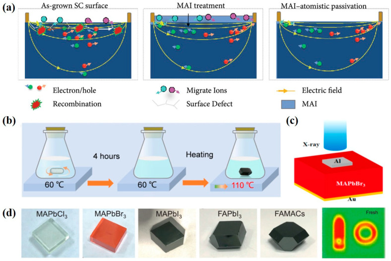
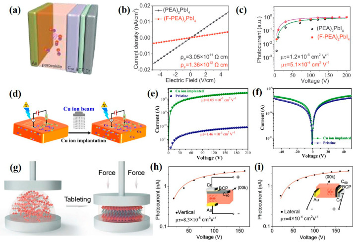
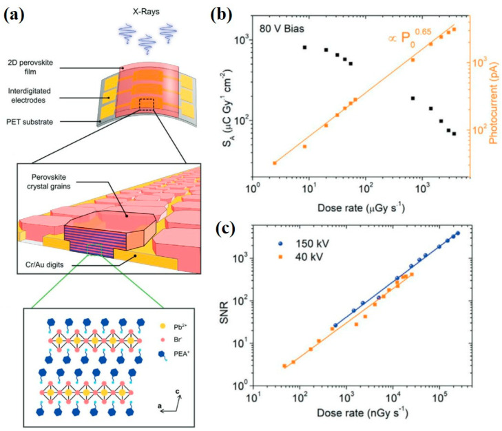
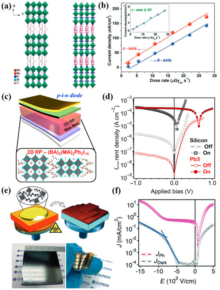
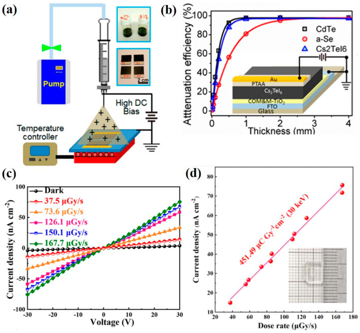
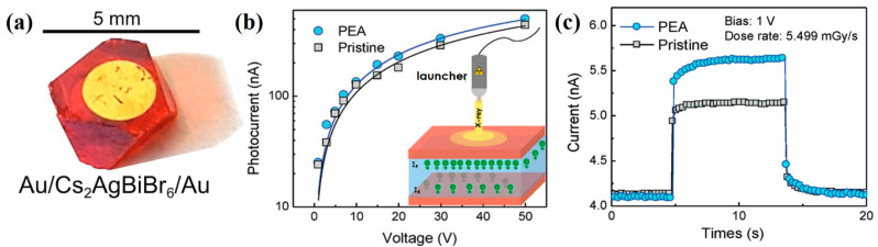
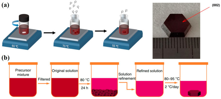
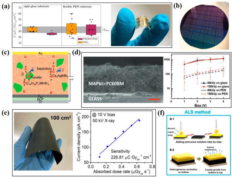
X-ray detection has widespread applications in medical diagnosis, non-destructive industrial radiography and safety inspection, and especially, medical diagnosis realized by medical X-ray detectors is presenting an increasing demand. Perovskite materials are excellent candidates for high-energy radiation detection based on their promising material properties such as excellent carrier transport capability and high effective atomic number. In this review paper, we introduce X-ray detectors using all kinds of halide perovskite materials along with various crystal structures and discuss their device performance in detail. Single-crystal perovskite was first fabricated as an active material for X-ray detectors, having excellent performance under X-ray illumination due to its superior photoelectric properties of X-ray attenuation with μm thickness. The X-ray detector based on inorganic perovskite shows good environmental stability and high X-ray sensitivity. Owing to anisotropic carrier transport capability, two-dimensional layered perovskites with a preferred orientation parallel to the substrate can effectively suppress the dark current of the device despite poor light response to X-rays, resulting in lower sensitivity for the device. Double perovskite applied for X-ray detectors shows better attenuation of X-rays due to the introduction of high-atomic-numbered elements. Additionally, its stable crystal structure can effectively lower the dark current of X-ray detectors. Environmentally friendly lead-free perovskite exhibits potential application in X-ray detectors by virtue of its high attenuation of X-rays. In the last section, we specifically introduce the up-scaling process technology for fabricating large-area and thick perovskite films for X-ray detectors, which is critical for the commercialization and mass production of perovskite-based X-ray detectors.

Keywords: X-ray detector; double perovskite; inorganic perovskite; lead-free perovskite; perovskite; photoelectronic effect; two-dimensional layered perovskite.


Conflict of interest statement

The authors declare no conflict of interest.

Figures

Figure 1
Figure 1
Application of organic–inorganic hybrid perovskite SCs in X-ray detectors. (a) Schematic diagram of the working principle for the X-ray detector with different surface treatments [31]. (b) Schematic diagram of the crystallization process for the MAPbI3 SCs with small and large temperature gradients [35]. (c) Schematic diagram of a device with Au/MAPbBr3 SCs/Al architecture [38]. (d) Different perovskite SCs fabricated by thermal evaporation and X-ray images of a closed black plastic box measured by the FAMACs-SC-based X-ray detector [41].
Figure 2
Figure 2
(a) Device structure, (b) dark current density and (c) photocurrent of self-powered X-ray detector based on 2D (F-PEA)2PbI4 perovskite [53]. (d) Schematic diagram of Cu ion implantation on the (PMA)2PbI4-based X-ray detector. (e) Sensitivity and (f) detection limit of (PMA)2PbI4-based X-ray detector after ion implantation [54]. (g) Schematic diagram of tableting process for the (F-PEA)3BiI6 SCs. Photocurrent of X-ray detector using (F-PEA)3BiI6 single crystal under (h) vertical and (i) horizontal electric fields [55].
Figure 3
Figure 3
(a) Photoconductor-type X-ray detectors by deposition of 2D PEA2PbBr4 micro-crystalline films on a flexible PET substrate. (b) Sensitivity per unit area (SA, black curve) and photocurrent (orange curve) as a function of dose rate. (c) SNR as a function of dose rate for the device under 150 kVp (blue curve) and 40 kVp (orange curve) accelerating voltages [51].
Figure 4
Figure 4
(a) Crystal structure of the quasi-2D BA2EA2Pb3Br10 perovskite. (b) X-ray-generated photocurrent of BA2EA2Pb3Br10 perovskite at various dose rates at a bias of 10 V [56]. (c) A p–i–n device architecture and (d) J–V curve of X-ray detector based on quasi-2D (BA)2(MA)2Pb3I10 perovskite [57]. (e) Fabrication process of thick film growth of quasi-2D perovskite and (f) J–V curve of corresponding X-ray detector [58].
Figure 5
Figure 5
(a) Schematic illustration of electrostatic-assisted spray coating process for deposition of large-area Cs2TeI6 perovskite. (b) Comparison of attenuation efficiency of CdTe, a-Se and Cs2TeI6 with different thicknesses for X-ray irradiation. Inset illustrates the device structure [60]. (c) J–V curves and (d) photocurrent as a function of dose rate of X-ray detector using Cs4PbI6 single crystal [61].
Figure 6
Figure 6
(a) Photo of X-ray detector with a device architecture of Au/Cs2AgBiBr6 perovskite/Au [62]. (b) I–V curves of X-ray detectors using pristine Cs2AgBiBr6 and PEA-Cs2AgBiBr6 single-crystal. (c) X-ray response of the Cs2AgBiBr6- and PEA-Cs2AgBiBr6-based devices [64].
Figure 7
Figure 7
(a) FA3Bi2I9 single crystal synthesized by the solution method through controlling the growth mechanism [67]. (b) Schematic diagram of preparation of the Cs3Bi2I9 single crystals by the nucleation-controlled solution method [68].
Figure 8
Figure 8
Application of large-area perovskite film for X-ray detectors. (a) Reliability of sensitivity for X-ray detectors fabricated on rigid and flexible substrates [69]. (b) Photo of large-area CsPbBr3 quantum dots deposited on TFT array [70]. (c) Illustration of working principle of X-ray detector using mixed Cs2AgBiBr6/(C36H34P2)MnBr4 scintillator [71]. (d) Cross-sectional SEM and X-ray photo-response of the device with bar coating of MAPbI3:PC60BM mixed absorber [72]. (e) Large-area lead-free Cs2TeI6 perovskite fabricated by electro-spraying on flexible substrates and the relationship between the photocurrent density of Cs2TeI6-based device and the exposure dose rate [73]. (f) Schematic illustration of the perovskite layer prepared by the ALS process [74].

Similar articles

Cited by

References

    1. Hoheisel M. Review of medical imaging with emphasis on X-ray detectors. Nucl. Instrum. Methods Phys. Res. Sect. A Accel. Spectrom. Detect. Assoc. Equip. 2006;563:215–224. doi: 10.1016/j.nima.2006.01.123. - DOI
    1. Zhou Y., Chen J., Bakr O.M., Mohammed O.F. Metal Halide Perovskites for X-ray Imaging Scintillators and Detectors. ACS Energy Lett. 2021;6:739–768. doi: 10.1021/acsenergylett.0c02430. - DOI
    1. Nikl M., Yoshikawa A. Recent R&D Trends in Inorganic Single-Crystal Scintillator Materials for Radiation Detection. Adv. Opt. Mater. 2015;3:463–481.
    1. Weber M.J. Inorganic scintillators: Today and tomorrow. J. Lumin. 2002;100:35–45. doi: 10.1016/S0022-2313(02)00423-4. - DOI
    1. Maddalena F., Xie A., Arramel, Witkowski M.E., Makowski M., Mahler B., Drozdowski W., Mariyappan T., Springham S.V., Coquet P., et al. Effect of commensurate lithium doping on the scintillation of two-dimensional perovskite crystals. J. Mater. Chem. C. 2021;9:2504–2512. doi: 10.1039/D0TC05647B. - DOI

LinkOut - more resources