. 2023 Aug;620(7975):756-761.
doi: 10.1038/s41586-023-06264-5. Epub 2023 Jul 19.

Mixing of moiré-surface and bulk states in graphite

Affiliations

Mixing of moiré-surface and bulk states in graphite

Ciaran Mullan et al. Nature. 2023 Aug.

Abstract

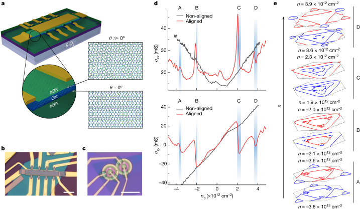
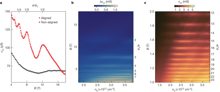
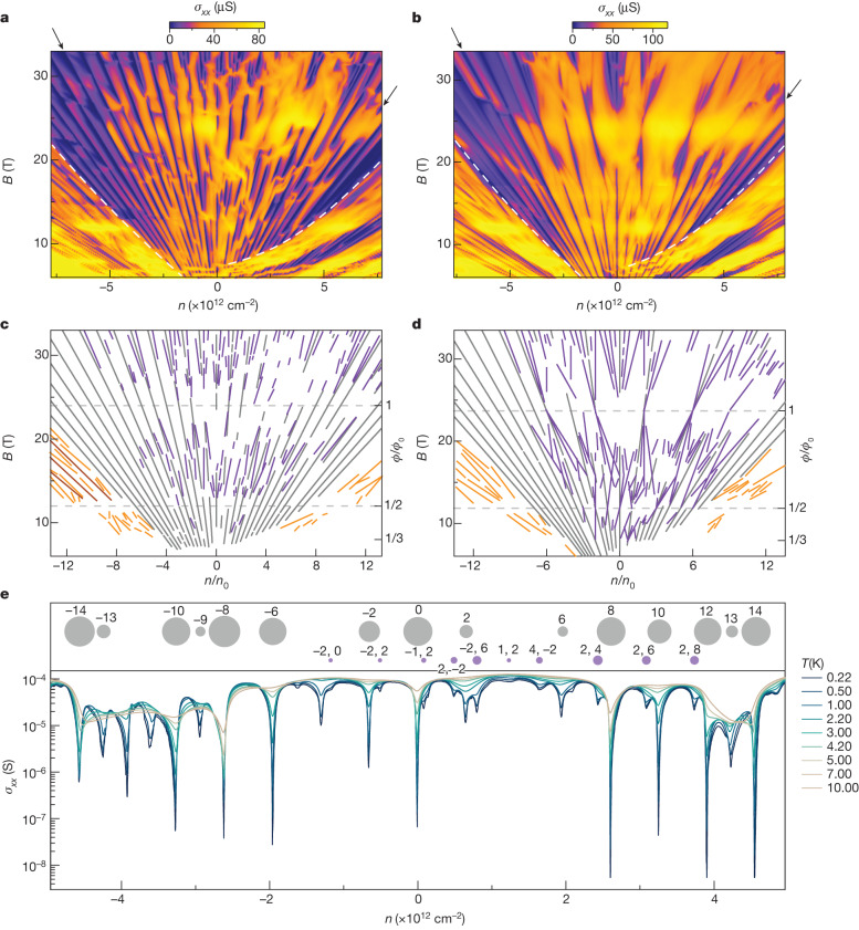
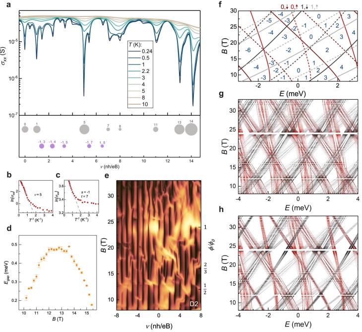
Van der Waals assembly enables the design of electronic states in two-dimensional (2D) materials, often by superimposing a long-wavelength periodic potential on a crystal lattice using moiré superlattices1-9. This twistronics approach has resulted in numerous previously undescribed physics, including strong correlations and superconductivity in twisted bilayer graphene10-12, resonant excitons, charge ordering and Wigner crystallization in transition-metal chalcogenide moiré structures13-18 and Hofstadter's butterfly spectra and Brown-Zak quantum oscillations in graphene superlattices19-22. Moreover, twistronics has been used to modify near-surface states at the interface between van der Waals crystals23,24. Here we show that electronic states in three-dimensional (3D) crystals such as graphite can be tuned by a superlattice potential occurring at the interface with another crystal-namely, crystallographically aligned hexagonal boron nitride. This alignment results in several Lifshitz transitions and Brown-Zak oscillations arising from near-surface states, whereas, in high magnetic fields, fractal states of Hofstadter's butterfly draw deep into the bulk of graphite. Our work shows a way in which 3D spectra can be controlled using the approach of 2D twistronics.


Conflict of interest statement

The authors declare no competing interests.

Figures

Fig. 1
Fig. 1. Moiré superlattice at the graphite–hBN interface.
a, Schematic of a heterostructure device with graphite (labelled Grt) encapsulated in hBN with one of the interfaces aligned. Here the lattice mismatch between graphite and hBN has been exaggerated for clarity. b,c, Optical micrographs of devices D1 (b) and D3 (c). Scale bar, 10 μm (b and c). d, Conductivities σxx and σxy as a function of the carrier density induced by the bottom gate, nb, for aligned device D1 and non-aligned device D4, measured at T = 0.24 K and non-quantizing B = 120 mT. e, Line cuts through the calculated dispersion relation in the kxky plane of the SBZ, at carrier densities (bottom to top) n (×1012 cm−2) = −3.8, −3.6, −2.1, −2.0, 1.9, 2.3, 3.6 and 3.9, grouped as pairs. Labels A, B, C and D correspond to the regions highlighted in d. The black dashed hexagon denotes the boundary of the first SBZ and red curves denote the hole and blue curves denote electron Fermi-surface cuts. Some lines at the corners are extended into the second SBZ for clarity.
Fig. 2
Fig. 2. BrownZak oscillations arising from surface states at the graphite–hBN interface.
a, Conductivity σxx as a function of B for device D2 at high electron concentrations induced by the top and bottom gates that dope the aligned and non-aligned graphite–hBN interfaces, respectively. For doping of the aligned interface, peaks appear at values of B equivalent to one flux quantum per q superlattice unit cells. nt = 3.1 × 1012 cm−2 and nb = 3.1 × 1012 cm−2 for aligned and non-aligned interfaces, respectively. T = 60 K. b, Conductivity map (a smooth background subtracted, see Methods, ‘Surface states in graphite films in the presence of a moiré superlattice’) as a function of B and nb at the aligned graphite–hBN interface of device D1. Measurements were performed at 60 K to suppress Landau quantization. The right y axis denotes the inverse flux ϕ0/ϕ. c, σxx(nb,B) map for the same device at 20 K.
Fig. 3
Fig. 3. Fractal 2.5D QHE states in graphite.
a,b, Conductivity σxx as a function of n = nt + nb and B for devices D2 (a) and D3 (b), T = 30 mK and nt = nb (that is, zero displacement field). The white dashed curves indicate the transition from surface Landau levels to the bulk UQR. Black arrows point to the threshold filling factors that bound the region of bulk in which fractal states are observed (ν = −9 and 12). c,d, Associated Wannier diagrams for panels a (c) and b (d): 2D QHE (grey) and fractal 2.5D QHE (purple) states in the UQR. The x axis is in units of n0 = 1/A0. Below UQR, orange lines trace fractal states and brown lines trace non-fractal states in the surface Landau levels +2 and −2. e, Hierarchy of 2.5D QHE gaps in aligned hBN/graphite/hBN. Bottom, σxx(n) traces at different T for device D3 at B = 13.5 T, which are used to extract gap sizes from Arrhenius activation. Top, bubble plot of the QHE gaps in which the area of circles scales linearly with the found gap sizes (ranging from 30 μeV to 1.8 meV). Grey and purple colour coding is the same as in d and labels are integers s and t from equation (1) for standard QHE (t only) and fractal QHE (s, t) states.
Fig. 4
Fig. 4. Hofstadter broadening of energy levels in graphite.
a, Hofstadter’s butterfly calculated for a honeycomb lattice following ref. , with a normalized energy scale. The dashed line marks ϕ/ϕ0 equivalent to B = 13.5 T, the field strength as in Fig. 3e. b, Landau levels resulting from quantized states from 0 Landau bands are shown in red and 1 Landau bands are shown in grey and calculated for a 16-layer-thick graphite film without a moiré perturbation. Zeeman splitting is included, as indicated by lighter and darker curves for the spin up and down, respectively. Labels in black refer to the filling factor ν. c, Expected spectra by applying Hofstadter’s butterfly in a as a small perturbation to each Landau level in b. Same labelling as in b. d, Conductivity map replotted from Fig. 3b as a function of ν. Two prominent gap closures around ϕ/ϕ0 = 1 have been labelled by the Landau band origin and spin of the levels that are crossing; the same colour coding as in b,c. Colour scale: brown to yellow, 0 μS to 115 μS.
Extended Data Fig. 1
Extended Data Fig. 1. DoS spectroscopy of surface states of graphite in zero magnetic field.
a, Capacitance (C) vs carrier density (n) for device D6 at T = 0.3 K. Inset shows optical micrograph of a typical capacitor device, scale bar 20 µm. b, Density of states (DoS) and quantum capacitance (Cq) vs surface potential (U1) from calculations based on effective-mass model (black line). Coloured symbols are experimental data from four different devices (D5, D6, D8, D11). Inset is calculated U1 vs n. c–f, Calculated dispersions of a 20-layer-thick graphite film for hole/electron dopings n = −6, −4, 4, 6 × 1012 cm−2 as a function of in-plane momentum kx,ky (horizontal axes) and energy E (vertical axis). Red (green) colour indicates surface states having high probability density of the wavefunction at the first (second) graphene bilayer. Upper outer surfaces with larger radius correspond to Type 1, and lower inner surface with a smaller radius correspond to Type 2. Blue colour indicates bulk states, and yellow contour highlights the Fermi level. g, same as c–f, calculated for zero doping where no distinct surface states are observed. h,i, Dispersion for propagating (Im kz = 0, black lines) and evanescent modes (Im kz ≠ 0, orange lines) for bulk graphite as a function of complex kz for fixed ħνk = 0.04 eV (panel h, 1D metal regime with Type 2 evanescent modes) and 0.15 eV (panel i, 1D semiconductor regime with Type 1 evanescent modes), respectively. Fermi level is at 0 eV. Green/blue arrows indicate evolution of surface states from propagating modes into evanescent modes for electron/hole doping.
Extended Data Fig. 2
Extended Data Fig. 2. Transport in aligned vs non-aligned interfaces at small magnetic fields.
a, c, σxx,σxy as a function of B and nb for aligned device D1 at T = 0.24 K. Landau level features emanate from LTs (|n| ≈ 2.0 and 3.7 × 1012 cm−2) and from zero doping. b, d, σxx,σxy as a function of B and nb for non-aligned device D4 at T = 0.22 K. e, Comparison of low field σxx line traces for the two interfaces of the single aligned D1, where aligned interface (nb) hosts many features related to the LTs which are notably absent in non-aligned interface (nt) response. f, Mapping of σxx for D1 as a function of nb and nt, highlighting that the vertical features related to LTs are independent of nt throughout the measured range. B = 0.3 T, T = 1.8 K, and the colour scale is black to white, 5 to 18 mS.
Extended Data Fig. 3
Extended Data Fig. 3. Brown-Zak mappings in aligned devices.
a, Extended range plot of Fig. 2b in the main text for device D1; ∆σxx (conductivity minus a smooth background) as a function of B and nb at T = 60 K. Inset, σxx(ϕ0/ϕ) trace at nb = 3.53 × 1012 cm−2 highlighting higher order Brown-Zak oscillation at ϕ0/ϕ = 5/2. b, Extended range plot of Fig. 2c in the main text; σxx as a function of B and nb at T = 20 K. Inset, conductivity averaged across a carrier density range nb = 2.00 to 3.84 × 1012 cm−2, ‹σxx(nb)›, plotted as a function of ϕ0/ϕ showing oscillations continuing down to experimental mapping resolution (Bstep = 1 mT). c–h High temperature mappings of σxx(nt, B) (panels c & g) and σxx(nb, B) (panels d & h) for doubly aligned device D3 (cd) and singly aligned device D2 (gh). Measurements were conducted at T = 60 K, colour scale black to white is 80 to 190 µS for c & d, 49 to 154 µS for g and 64 to 97 µS for h. Panels e & f show 1st and 2nd derivatives, respectively, calculated from d. Horizontal dashed lines show the significant flux fractions ϕ/ϕ0 from 1/2 to 1/8 fitted to the data. Colour scale for e is blue to red −40 to 40 µS T−1 and in f is black to white −100 to 100 µS T−2.
Extended Data Fig. 4
Extended Data Fig. 4. Classical interpretation of Brown-Zak oscillations and conductivity enhancement.
a, Dispersion in the SBZ plotted up to Fermi energy for doping 2.1 × 1012 cm2 (left) and 3.8 × 1012 cm2 (right) respectively. b, networks of classical trajectories accessible to surface state electrons at the same dopings in a. Examples of shortest interfering paths of equal length are shown by green and brown arrows. The area enclosed between these paths equals ABZ/(eB)2 irrespective of energy. c, Conductivity enhancement at high B field in aligned Corbino devices; σxx as a function of single gate induced carrier density for non-aligned device (D10, black curve, bottom gate tuned), singly aligned device (D2, red curve, top gate tuned) and doubly aligned device (D3, blue curve, bottom gate tuned) all in Corbino geometry, measured at T = 0.3 K and B = 18 T. Shaded regions highlight surface Landau band features. d, Conductivity at zero B field in aligned (D1) vs non-aligned (D9) Hall bar devices. Increased scattering due to alignment results in reduced conductivity in the bulk at B = 0 T. Here the top (non-aligned interface) gate is swept for D1. T = 0.3 K. e, Brown-Zak oscillations in σxx differ in amplitude non-monotonically as a function of ϕ0/ϕ in aligned Hall bar device D1. Measured at nb = 2.6 × 1012 cm−2, where T = 60 K curve is from the same dataset used to generate Fig. 2b and Extended Data Fig. 2a.
Extended Data Fig. 5
Extended Data Fig. 5. Existence of fractal states throughout the bulk.
a, σxx(nt, nb) of device D2 as a function of top and bottom gates, nb and nt, measured at high field B = 15.6 T, T = 0.3 K, colour scale: brown to yellow, 0 to 59 μS. b, Wannier diagram depicting the QHE and fractal QHE gaps in the bulk as diagonal grey and purple lines, respectively. High doping for top (bottom) gate results in horizontal (vertical) features that correspond to surface states accessing the +2 and −2 Landau bands from the opposite graphite surfaces (highlighted by orange shading). c, σxx(nt, nb) of device D3, measured at high field B = 13.6 T, T = 0.3 K, colour scale: brown to yellow, 0 to 98 μS. d, The same as b but for D3.
Extended Data Fig. 6
Extended Data Fig. 6. Gap size hierarchy in device D2.
a, Upper panel, σxx as a function of integer QHE filling factor ν at various temperatures, B = 15.2 T. Lower panel, bubble plot of extracted gap size from Arrhenius fits to the σxx minima. Gap size scales with area (60 µeV to 0.9 meV), and grey bubbles are integer gaps (labelled by ν) and purple bubbles are fractal gaps (labelled by s, t). b,c, Examples of Arrhenius plots of ln[σxx] as a function of reciprocal temperature for integer QHE gap at ν = 5 and fractal QHE gap of integers (s,t) = (−1,7), respectively. The linear regions are fitted to yield a slope of ≈ ½Egap. d, Gap size extracted from Arrhenius fits as a function of B for the ν = 0 gap. e, Conductivity map for device D2, same data as in Fig. 3a in the main text, except plotted as a function of filling factor ν of main QHE sequence. Colour scale: brown to yellow, 0 to 80 μS. f, Allowed energy levels resulting from quantised states from 0 (1) Landau bands shown in red (grey), calculated for 21-layer-thick graphite film without a moiré perturbation. Zeeman splitting has been included, as indicated by light and dark lines for spin up and spin down, respectively. g, Combination of panels f and Fig. 4a in the main text by applying Hofstadter’s butterfly as a small perturbation (S = 0.42 meV) to each energy level, Eq. 2. h, Same as g but with S = 0.42 meV for odd layer states and S = 0.12 meV for even layer states.
Extended Data Fig. 7
Extended Data Fig. 7. Magnetocapacitance oscillations and Landau fan diagram of the surface states.
a, Typical C(n) at 0.6 T (bottom black curve), 5.1 T (middle blue curve) and 12 T (top red curve), respectively, in capacitor device D6 at T = 0.3 K. Bottom insets are magnifications of the marked areas. b, DoS vs U1 at 5.1 T, 0.3 K. c, Surface Landau fan diagram C (n, B) at 0.3 K. Colour scale: navy to white, 254.7 fF to 270.0 fF. Dashed line marks the critical field B = 7.5 T, where bulk Landau band 2+ leaves the Fermi level and graphite enters the UQR. d, Dispersion relation for bulk Landau bands calculated using the SWMC model at B = 7.5 T.
Extended Data Fig. 8
Extended Data Fig. 8. Low field quantum oscillations.
a, Oscillations of Δρxx in device D7 obtained by subtracting a smooth background while sweeping the gate voltage (Vb) at 0.1 T, 0.3 K using excitation I = 1 μA. The encapsulated graphite with a thickness of 20 nm is defined to Hall bar geometry for this measurement. b, dns/dn as a function of n at 0.6 T, where ns is the carrier density injected into the surface states, n is the total electrostatically induced carrier density. It is deduced from the curve shown in Extended Data Fig. 7a, based on the periodicity of the oscillations.
Extended Data Fig. 9
Extended Data Fig. 9. Fractional surface states in non-aligned graphite.
a,b, Fractional surface states measured in capacitance (device D8). a, C(n) at B = 20 T, T = 0.3 K. Inset magnifies the encircled region, but plots as C(ν). b, dC/dν (ν, B) of S2+ in high B region. Colour scale: blue to red, −6 to 6 fF. Right-top inset shows the corresponding C (n, B) map. Colour scale: orange to red, 254.3 to 260 fF. c, Longitudinal conductivity σxx (B, n) measured at D = 0.24 V/nm in a Hall bar device D9, T = 0.3 K, I = 20 nA. The white shaded areas are guides to the eye for the surface states. Boundaries of one such surface states are marked by white dotted curves. Logarithmic colour scale: navy to orange, 0.1 to 118.2 µS. d, σxx cut profile (black curve) of the white dashed line in c and the corresponding Hall conductivity σxy (red curve).
Extended Data Fig. 10
Extended Data Fig. 10. Raman characterization of aligned and non-aligned ABA graphite.
a, Optical image and b, AFM profile of graphite flake used in Raman measurement (area shown in the black box in a). The flake contains both regions of MLG and graphite with thickness around 10 layers. Scale bar 10 um. c, Optical image of the stack fabricated for Raman measurements. The aligned and non-aligned regions are marked by blue and red dashed lines. Scale bar 10 um. d, Raman map of full width half maximum (FWHM) of 2D peak. The MLG and graphite regions are colour-coded in grayscale and red-to-purple, respectively. e, Comparison of 2D peak between aligned and non-aligned regions in MLG (up) and graphite (down). Each spectrum shown here is averaged over ten spectra at different spots. The intensity is normalized by that of hBN peak at 1363 cm−1.

References

    1. Mak KF, Shan J. Semiconductor moiré materials. Nat. Nanotechnol. 2022;17:686–695. doi: 10.1038/s41565-022-01165-6. - DOI - PubMed
    1. Lau CN, Bockrath MW, Mak KF, Zhang F. Reproducibility in the fabrication and physics of moire materials. Nature. 2022;602:41–50. doi: 10.1038/s41586-021-04173-z. - DOI - PubMed
    1. Ciarrocchi A, Tagarelli F, Avsar A, Kis A. Excitonic devices with van der Waals heterostructures: valleytronics meets twistronics. Nat. Rev. Mater. 2022;7:449–464. doi: 10.1038/s41578-021-00408-7. - DOI
    1. Liu Y, et al. Moiré superlattices and related moiré excitons in twisted van der Waals heterostructures. Chem. Soc. Rev. 2021;50:6401–6422. doi: 10.1039/D0CS01002B. - DOI - PubMed
    1. Kennes DM, et al. Moiré heterostructures as a condensed-matter quantum simulator. Nat. Phys. 2021;17:155–163. doi: 10.1038/s41567-020-01154-3. - DOI