Effects of surface properties of GaN semiconductors on cell behavior
- PMID: 37496912
- PMCID: PMC10366471
- DOI: 10.1016/j.heliyon.2023.e18150
Effects of surface properties of GaN semiconductors on cell behavior
Abstract
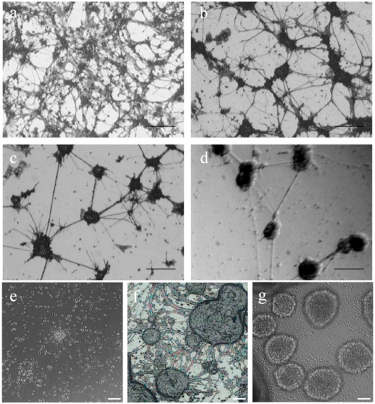
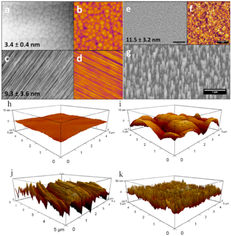
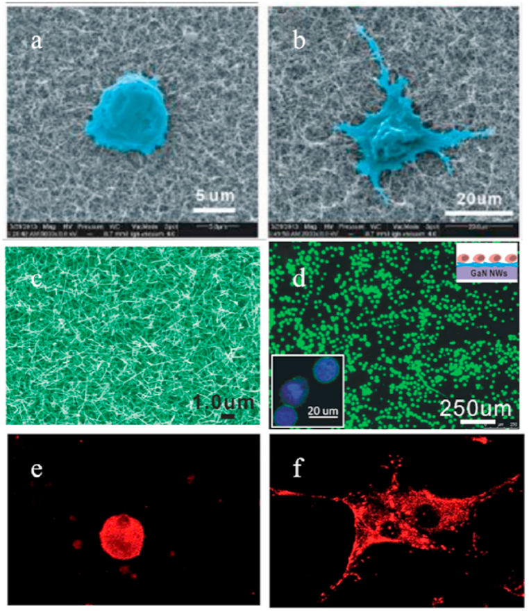
In recent years, semiconductors have aroused great interest in connecting, observing and influencing the behavior of biological elements, and it is possible to use semiconductor-cell compound interfaces to discover new signal transduction in the biological field. Among them, III-V nitride semiconductors, represented by gallium nitride (GaN), are used as substrates to form semiconductor-biology interfaces with cells, providing a platform for studying the effects of semiconductors on cell behavior. The interfaces between GaN substrate and cells play an important role in detecting and manipulating cell behaviors and provide a new opportunity for studying cell behavior and developing diagnostic systems. Hence, it is necessary to understand how the properties of the GaN substrate directly influence the behavior of biological tissues, and to create editable biological interfaces according to the needs. This paper reviews the synergism between GaN semiconductors and biological cells. The electrical properties, persistent photoconductivity (PPC), nanostructures, and chemical functionalization of GaN on the promotion of cell behaviors, such as growth, adhesion, differentiation, and signal transduction, are emphatically introduced. The purpose of this study is to provide guidance to explore the detection and regulation methods of cell behavior based on semiconductors and promote the application of them in the field of bioelectronics, such as biochips, biosensors, and implantable systems.
Keywords: Bioelectronics; Cell; GaN; Interface; Semiconductor; Surface.
© 2023 Published by Elsevier Ltd.
Conflict of interest statement
The authors declare that they have no known competing financial interests or personal relationships that could have appeared to influence the work reported in this paper.
Figures


Similar articles
-
Investigation of Persistent Photoconductivity of Gallium Nitride Semiconductor and Differentiation of Primary Neural Stem Cells.Molecules. 2024 Sep 19;29(18):4439. doi: 10.3390/molecules29184439. Molecules. 2024. PMID: 39339434 Free PMC article.
-
Enhanced cell growth on nanotextured GaN surface treated by UV illumination and fibronectin adsorption.Colloids Surf B Biointerfaces. 2014 Nov 1;123:293-301. doi: 10.1016/j.colsurfb.2014.09.030. Epub 2014 Sep 22. Colloids Surf B Biointerfaces. 2014. PMID: 25264283
-
Persistent Photoconductivity, Nanoscale Topography, and Chemical Functionalization Can Collectively Influence the Behavior of PC12 Cells on Wide Bandgap Semiconductor Surfaces.Small. 2017 Jun;13(24). doi: 10.1002/smll.201700481. Epub 2017 May 2. Small. 2017. PMID: 28464526
-
Electronic Biosensors Based on III-Nitride Semiconductors.Annu Rev Anal Chem (Palo Alto Calif). 2015;8:149-69. doi: 10.1146/annurev-anchem-071114-040247. Epub 2015 May 27. Annu Rev Anal Chem (Palo Alto Calif). 2015. PMID: 26048553 Review.
-
Hydrostatic Pressure as a Tool for the Study of Semiconductor Properties-An Example of III-V Nitrides.Materials (Basel). 2024 Aug 13;17(16):4022. doi: 10.3390/ma17164022. Materials (Basel). 2024. PMID: 39203200 Free PMC article. Review.
Cited by
-
Pros and Cons of (NH4)2S Solution Treatment of p-GaN/Metallization Interface: Perspectives for Laser Diode.Materials (Basel). 2024 Sep 14;17(18):4520. doi: 10.3390/ma17184520. Materials (Basel). 2024. PMID: 39336261 Free PMC article.
References
-
- Ling W., Yu J., Ma N., et al. Flexible electronics and materials for synchronized stimulation and monitoring in multi-encephalic regions. Adv. Funct. Mater. 2020;30 doi: 10.1002/adfm.202002644. - DOI
-
- Kang B.S., Wang H.T., Lele T.P., Tseng Y., Ren F., Pearton S.J., Johnson J.W., Rajagopal P., Roberts J.C., Piner E.L., Linthicum K.J. Prostate specific antigen detection using AlGaN∕GaN high electron mobility transistors. Appl. Phys. Lett. 2007;91 doi: 10.1063/1.2772192. - DOI
-
- Chen K.H., Kang B.S., Wang H.T., Lele T.P., Ren F., Wang Y.L., Chang C.Y., Pearton S.J., Dennis D.M., Johnson J.W., Rajagopal P., Roberts J.C., Piner E.L., Linthicum K.J. c-erbB-2 sensing using AlGaN∕GaN high electron mobility transistors for breast cancer detection. Appl. Phys. Lett. 2008;92 doi: 10.1063/1.2926656. - DOI
-
- Steinhoff G., Baur B., Wrobel G., Ingebrandt S., Offenhäusser A., Dadgar A., Krost A., Stutzmann M., Eickhoff M. Erratum: recording of cell action potentials with AlGaN∕GaN field-effect transistors. Appl. Phys. Lett. 2006;89 doi: 10.1063/1.2219129. - DOI
Publication types
LinkOut - more resources
Full Text Sources