Review
. 2023 Jul 8;14(7):1393.
doi: 10.3390/mi14071393.

Metallic and Non-Metallic Plasmonic Nanostructures for LSPR Sensors

Affiliations
Review

Metallic and Non-Metallic Plasmonic Nanostructures for LSPR Sensors

Judy Z Wu et al. Micromachines (Basel). .

Abstract

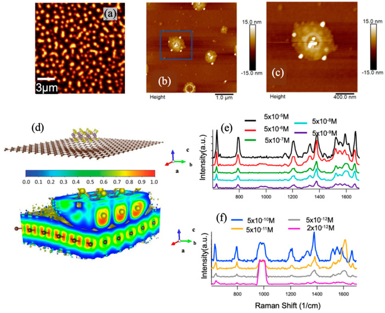
Localized surface plasmonic resonance (LSPR) provides a unique scheme for light management and has been demonstrated across a large variety of metallic nanostructures. More recently, non-metallic nanostructures of two-dimensional atomic materials and heterostructures have emerged as a promising, low-cost alternative in order to generate strong LSPR. In this paper, a review of the recent progress made on non-metallic LSPR nanostructures will be provided in comparison with their metallic counterparts. A few applications in optoelectronics and sensors will be highlighted. In addition, the remaining challenges and future perspectives will be discussed.

Keywords: 2D materials; LSPR; SERS; graphene; high sensitivity; plasmonic nanostructures.


Conflict of interest statement

The authors declare no conflict of interest.

Figures

Figure 3
Figure 3
(a) Schematic description of R6G molecules attached on Au nanoparticles/graphene SERS substrate. Reproduced with permission [39]. Copyright 2015, Elsevier. (b) Schematic description of the SERS process with graphene-enhanced CM effect.
Figure 8
Figure 8
(a) Device structure of a CH3NH3PbI3/graphene/AuNPs hybrid photodetector. Reproduced with permission from Ref. [89]. Copyright 2009, Royal Society of Chemistry. (b) Device configuration of a CH3NH3PbI3/AuNPs hybrid photodetector. Reproduced with permission from Ref. [90]. Copyright 2018, Wiley. (c) Schematic diagrams of a metal NP embed in a perovskite thin film with a direct contact to perovskite, and a metal NP embedded in a SiO2 metafilm with a perovskite thin film atop. The yellow arrows represent incident light on the perovskite. The charge, energy and heat transfer effects are illustrated by green, blue and orange arrows, respectively, which can be effectively suppressed using the AgNPs embedded silica metafilm. (d) Schematic structure of a perovskite/graphene heterojunction photodetector on AgNPs-silica metafilm. Reproduced with permission from Ref. [94]. Copyright 2019, American Chemical Society. (e) Schematic image of AuCu/CsPbCl3 core/shell/graphene hybrid photodetectors with LSPR enhanced photoresponsivity. Reproduced with permission from Ref. [95]. Copyright 2020, Wiley. (f) Schematic illustration of the graphene/WS2-ND/AgNP metafilm heterostructure photodetector Reproduced with permission from Ref. [96]. Copyright 2019, American Chemical Society.
Figure 1
Figure 1
Schematic description of LSPR in metallic NPs through oscillation of free electrons on the NP surface.
Figure 2
Figure 2
Localized surface plasmon resonance (LSPR) frequency dependence on free carrier density and doping constraints. The bottom panel shows the modulation of the LSPR frequency (ωsp) of a spherical nanoparticle by control of its free carrier concentration (N). LSPR frequency is estimated as: 1/2π (Ne2/(εome(ε+2εm). The high frequency dielectric constant ε is assumed to be 10, the medium dielectric constant εm is set as 2.25 for toluene, and the effective mass of the free carrier me is assumed to be that of a free electron. The e is the electronic charge and εo is the permittivity of free space. The top panel shows a calculation of the number of dopant atoms required for nanoparticle sizes ranging from 2 to 12 nm to achieve a free carrier density between 1017 and 1023 cm−3. For LSPRs in the visible region, a material in which every atom contributes a free carrier to the nanoparticle, as for metals, is required. For LSPRs in the infra-red, carrier densities of 1019–1022 cm−3 are required. Below 1019 cm−3, the number of carriers (for a 10 nm nanocrystal) may be too low (<10) to support an LSPR mode. The brown diamond indicates the region of interest in the present study. Reprint with permission of [13], Copyright 2011, Springer Nature.
Figure 4
Figure 4
Schematic depiction of the synthesis process: (a) wet transfer of graphene on SiO2/Si substrates (b,c) MoS2 synthetization on graphene via the vapor transport process. (d,e) Synthesis of the MoS2 nanostructures: N-disc at low (f) and N-donut at high (g) (NH4)2MoS4 precursor concentration with the hypothetical growth mechanism where triangles denote MoS2 nuclei produced during the vapor transport annealing procedure. Reproduced with permission [43]. Copyright 2021, MDPI.
Figure 5
Figure 5
(a) Raman map of MoS2 (using A1g mode). (b) Representative AFM images (5 μm×5 μm) of the sample with zoom in view (c). Reproduced with permission [43]. Copyright 2021, MDPI. (d) Vertical MoS2/graphene bilayer heterostructure (top) and the corresponding Electron Localization Function (ELF) (bottom) showing the localized electron concentration underneath the sulfur atom demonstrating the charge transfer occurrence. Reproduced with permission [41]. Copyright 2019, Wiley-VCH. (e) Raman spectra of the R6G molecules with different concentrations in the range of 5 × 10⁻⁵ M to 5 × 10⁻⁹ M (c), and (f) 5 × 10⁻¹⁰ M to 2 × 10⁻¹² M on the MoS2 N-donut/graphene vdW heterostructures substrates. All spectra were collected using 532 nm excitation. Reproduced with permission [43]. Copyright 2021, MDPI.
Figure 6
Figure 6
(a) 3D ELF plot of the stack of Au/WS2 heterostructure. Reproduced with permission [54]. Copyright 2019, ACS. (b) Graphene Raman spectra taken on four samples: graphene only, WS2NDs/graphene, AuNPs/graphene and AuNPs/WS2-NDs/graphene. (c) Raman map of WS2. (d) AFM image of the WS2-NDs; (e,f) an SEM image of an AuNPs/WS2-NDs/graphene sample and EDS maps of W, Au and C. (g) Raman spectra of R6G molecules with a concentration of 5 × 10⁻⁵ M on different substrates. Reproduced with permission [53]. Copyright 2020, ACS.
Figure 7
Figure 7
(a) Schematic description of AuNP/graphene SERS substrate with R6G probe molecules attached. (b) Comparison of Raman spectra of R6G probe molecules attached on four different substrates: AuNPs/graphene/SiO2/Si, AuNPs/SiO2/Si, graphene/SiO2/Si and bare SiO2/Si, respectively. Reproduced with permission [39]. Copyright 2015, Elsevier. (c) Raman spectra of R6G molecules at different concentrations in the range of 5 × 10⁻⁵ to 8 × 10⁻⁷ on AuNP/graphene SERS substrate. Reproduced with permission [24]. Copyright 2017, Elsevier. (d) Schematic description of graphene/AuNPs SERS substrates (top-left inset), and the Raman spectra of R6G molecules on the graphene/AuNP SERS substrates of concentrations in the range of 10−7 to 10−11. Reproduced with permission [52]. Copyright 2016, Elsevier. (e) Schematic diagram of MoS2/AgNPs hybrid system (f) Raman spectra of R6G molecules of different concentrations from 5 × 10⁻⁵ to 8 × 10⁻⁹. Reproduced with permission [58]. Copyright 2016, Elsevier. (g) Schematic showing the Au-WS2 nanohybrid SERS platform, (h) Raman spectra of R6G molecules using concentrations from 5 × 10⁻⁴ to 8 × 10⁻⁸ on Au-WS2 nanohybrid SERS. Reproduced with permission [59]. Copyright 2018, Microchimica Acta.

References

    1. Novoselov K.S., Geim A.K., Morozov S.V., Jiang D., Zhang Y., Dubonos S.V., Grigorieva I.V., Firsov A.A. Electric field effect in atomically thin carbon films. Science. 2004;306:666–669. doi: 10.1126/science.1102896. - DOI - PubMed
    1. Geim A.K., Novoselov K.S. The rise of graphene. Nat. Mater. 2007;6:183–191. doi: 10.1038/nmat1849. - DOI - PubMed
    1. Aroca R.F., Alvarez-Puebla R.A., Pieczonka N., Sanchez-Cortez S., Garcia-Ramos J.V. Surface-enhanced Raman scattering on colloidal nanostructures. Adv. Colloid Interface Sci. 2005;116:45–61. doi: 10.1016/j.cis.2005.04.007. - DOI - PubMed
    1. Baker G.A., Moore D.S. Progress in plasmonic engineering of surface-enhanced Raman-scattering substrates toward ultra-trace analysis. Anal. Bioanal. Chem. 2005;382:1751–1770. doi: 10.1007/s00216-005-3353-7. - DOI - PubMed
    1. Gunnarsson L., Bjerneld E.J., Xu H., Petronis S., Kasemo B., Käll M. Interparticle coupling effects in nanofabricated substrates for surface-enhanced Raman scattering. Appl. Phys. Lett. 2001;78:802–804. doi: 10.1063/1.1344225. - DOI

LinkOut - more resources