Review
. 2023 Jul 29;15(1):187.
doi: 10.1007/s40820-023-01161-y.

Multifunctional Perovskite Photodetectors: From Molecular-Scale Crystal Structure Design to Micro/Nano-scale Morphology Manipulation

Affiliations
Review

Multifunctional Perovskite Photodetectors: From Molecular-Scale Crystal Structure Design to Micro/Nano-scale Morphology Manipulation

Yingjie Zhao et al. Nanomicro Lett. .

Abstract

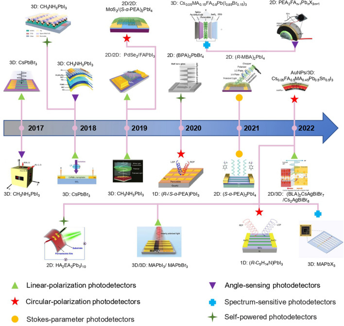
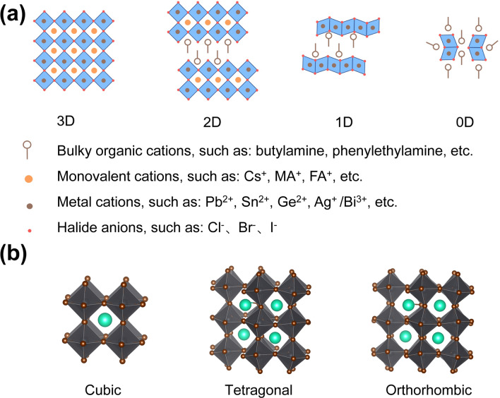
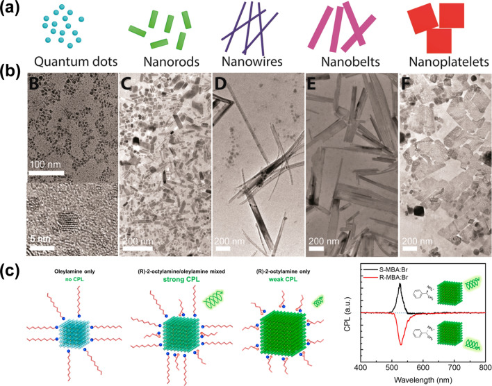
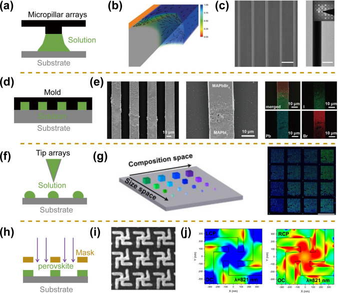
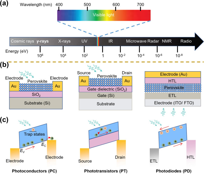
Multifunctional photodetectors boost the development of traditional optical communication technology and emerging artificial intelligence fields, such as robotics and autonomous driving. However, the current implementation of multifunctional detectors is based on the physical combination of optical lenses, gratings, and multiple photodetectors, the large size and its complex structure hinder the miniaturization, lightweight, and integration of devices. In contrast, perovskite materials have achieved remarkable progress in the field of multifunctional photodetectors due to their diverse crystal structures, simple morphology manipulation, and excellent optoelectronic properties. In this review, we first overview the crystal structures and morphology manipulation techniques of perovskite materials and then summarize the working mechanism and performance parameters of multifunctional photodetectors. Furthermore, the fabrication strategies of multifunctional perovskite photodetectors and their advancements are highlighted, including polarized light detection, spectral detection, angle-sensing detection, and self-powered detection. Finally, the existing problems of multifunctional detectors and the perspectives of their future development are presented.

Keywords: Crystal structure design; Micro/nano-structure manipulation; Multifunctional photodetectors; Perovskite materials; Working mechanism.


Conflict of interest statement

The authors declare no interest conflict. They have no known competing financial interests or personal relationships that could have appeared to influence the work reported in this paper.

Figures

Fig. 1
Fig. 1
Overview of the development of multifunctional perovskite photodetectors in recent years, mainly including polarized light detection [, , , , , , –64], spectral detection [27, 65], angle detection [54, 66, 67], and self-powered detection [68, 69]. Reproduced with permission from Ref. [21] Copyright 2019, Springer Nature; Reproduced with permission from Ref. [46] Copyright 2019, American Chemical Society; Reproduced with permission from Ref. [47] Copyright 2021, American Chemical Society; Reproduced with permission from Ref. [48] Copyright 2022, Wiley–VCH; Reproduced with permission from Ref. [49] Copyright 2018, The Royal Society of Chemistry; Reproduced with permission from Ref. [50] Copyright 2019, Springer Nature; Reproduced with permission from Ref. [51] Copyright 2022, Wiley–VCH; Reproduced with permission from Ref. [55] Copyright 2017, Wiley–VCH; Reproduced with permission from Ref. [56] Copyright 2020, Wiley–VCH; Reproduced with permission from Ref. [58] Copyright 2022, Elsevier; Reproduced with permission from Ref. [59] Copyright 2018, Wiley–VCH; Reproduced with permission from Ref. [60] Copyright 2019, Wiley–VCH; Reproduced with permission from Ref. [61] Copyright 2019, Wiley–VCH; Reproduced with permission from Ref. [62] Copyright 2021, Wiley–VCH; Reproduced with permission from Ref. [63] Copyright 2022, Wiley–VCH; Reproduced with permission from Ref. [64] Copyright 2022, Wiley–VCH; Reproduced with permission from Ref. [27] Copyright 2022, Wiley–VCH; Reproduced with permission from Ref. [65] Copyright 2021, Wiley–VCH; Reproduced with permission from Ref. [54] Copyright 2017, American Chemical Society; Reproduced with permission from Ref. [66] Copyright 2018, Wiley–VCH; Reproduced with permission from Ref. [67] Copyright 2022, Springer Nature; Reproduced with permission from Ref. [68] Copyright 2018, American Chemical Society; Reproduced with permission from Ref. [69] Copyright 2022, American Chemical Society
Fig. 2
Fig. 2
Classification of perovskite materials. a Diversity of perovskite materials, mainly including 3D, 2D, 1D, and 0D structures. b Crystal structures of perovskite materials
Fig. 3
Fig. 3
Morphology management of perovskite nanocrystals using hot-injection process. a Schematic diagram and b TEM images of perovskite nanocrystals with different shapes. Reproduced with permission from Ref. [74] Copyright 2019, American Chemical Society. c Schematic diagram and CPL of ligand-treated FAPbBr3 quantum dots. Reproduced with permission from Ref. [76] Copyright 2020, American Chemical Society
Fig. 4
Fig. 4
Morphology management of perovskites using different processing technology. a Schematic diagram of the capillary liquid bridge method. b Fluid simulation diagram of the capillary liquid bridge. c SEM and TEM images of perovskite nanowire arrays. Reproduced with permission from Ref. [55] Copyright 2017, Wiley–VCH. d Schematic diagram of PDMS template method. e SEM and EDS mapping images of perovskite heterojunction arrays. Reproduced with permission from Ref. [63] Copyright 2022, Wiley–VCH. f Schematic diagram of dip pen printing method. g Confocal PL mapping of 16 individual perovskite arrays. Reproduced with permission from Ref. [77] Copyright 2022, American Chemical Society. h Schematic diagram of etching technique. i SEM image of perovskite chiral metasurfaces. j Color maps showing dissimilar spatial distributions of optical chirality for a left-handed chiral gammadion meta molecule at different circular polarization illumination. Reproduced with permission from Ref. [78] Copyright 2022, Springer Nature
Fig. 5
Fig. 5
Classification of perovskite photodetectors. a The detection wavelength of photodetectors. b Device structures and c their operating mechanisms of perovskite photodetectors
Fig. 6
Fig. 6
Linearly polarized light detection. a Schematic diagram of layered perovskite crystals, (BA)2(MA)Pb2Br7. The red arrow represents the possible direction of electric polarization. b Angle-dependent photocurrent under different polarized light irradiation (left). Time-dependent photoresponse (right). Reproduced with permission from Ref. [81] Copyright 2019, American Chemical Society. c Schematic diagram of (202) crystallographically oriented 2D perovskite polycrystalline films, PEA2MA4(Sn0.5Pb0.5)5I16. d Polarized light imaging with the 0° polarization light (top) and 90° polarization light (bottom). Reproduced with permission from Ref. [85] Copyright 2021, Wiley–VCH. e Energy level diagram of two-photon absorption (left) and angle-dependent photocurrent under different polarized light irradiation (right). Reproduced with permission from Ref. [89] Copyright 2019, Wiley–VCH. f The optical photo (top) and cross-section image (bottom) of 2D/3D double perovskite heterojunctions. g Angle-dependent photocurrent under different polarized light irradiation. Reproduced with permission from Ref. [64] Copyright 2022, Wiley–VCH. h Schematic diagram of polarized photodetector based on MAPbBr3-MAPbI3 lateral heterojunctions. i Angle-dependent photocurrent under different polarized light irradiation. Reproduced with permission from Ref. [63] Copyright 2022, Wiley–VCH
Fig. 7
Fig. 7
Linearly polarized light detection. a Schematic diagram of the preparation process for 1D nano-grating structure atop a two-dimensional photonic crystal structure. b Schematic diagram of polarized light detector (left). Angle-dependent photocurrent under different polarized light irradiation (right). Reproduced with permission from Ref. [61] Copyright 2019, Wiley–VCH. c Schematic diagram of in-situ encapsulated Moiré lattice-perovskite films. d Angle-dependent I-V curves (left) and I-t curves (right) under different polarized light irradiation. Reproduced with permission from Ref. [88] Copyright 2022, Wiley–VCH. e Scanning electron microscope images (left) and schematic diagrams of the capillary trailing (right). f Schematic diagram of polarized light detector (left). Angle-dependent photocurrent under different polarized light irradiation (right). Reproduced with permission from Ref. [55] Copyright 2017, Wiley–VCH
Fig. 8
Fig. 8
Circularly polarized light detection. a Schematic diagram of the crystal structures. b CD and absorbance spectra of 1D (R-/S-rac-MBA)PbI3 perovskite films. c Wavelength-dependent responsivities under the excitation of different circularly polarized light. Reproduced with permission from Ref. [21] Copyright 2019, Springer Nature. d Schematic diagram of the crystal structure, [(R)-β-MPA]2MAPb2I7. e CD spectra of 2D perovskite films. f Voltage-dependent currents under right-handed circularly polarized (RCP) and left-handed circularly polarized (LCP) light at the wavelengths of 532 nm. Reproduced with permission from Ref. [110] Copyright 2020, Wiley–VCH
Fig. 9
Fig. 9
Circularly polarized light detection. a Preparation process of perovskite heterojunction. b Schematic diagram of circularly polarized light detection based on perovskite heterojunction. c Diagram of the working mechanism for a heterojunction photodetector. d Angle-dependent photocurrents under circularly polarized light irradiation with the different rotation angles of a λ/4 plate. Reproduced with permission from Ref. [125] Copyright 2022, American Chemical Society. e Schematic diagram of the interaction between AuNPs and perovskite (right) and its SEM image (left). f Schematic diagram of a flexible circularly polarized photodetector and its photograph (left). gres at different bending radii (right). Reproduced with permission from Ref. [51] Copyright 2022, Wiley–VCH
Fig. 10
Fig. 10
Stokes-parameter light detection. a Schematic diagram of the Stokes-parameter photodetector based on chiral perovskite nanowire arrays. b Theoretical absorption intensity for different Stokes parameters presented on the Poincare-spheré. c Experimental measurements and theoretically derived values for different states of polarized light. Reproduced with permission from Ref. [47] Copyright 2021, American Chemical Society. d Schematic diagram of the full-Stokes polarimeter based on chiral 2D perovskite single crystals. e Experimental measurements and input values for polarized light with different polarization states. Reproduced with permission from Ref. [62] Copyright 2021, Wiley–VCH
Fig. 11
Fig. 11
Spectrum-sensitive photodetectors. a Photographs of perovskite single crystals with different halide compositions. b Schematic diagram of narrow-band photodetectors. c Normalized external quantum efficiency pattern of perovskite single crystals with different halogen compositions, demonstrating the capability of narrow-band photodetection. Reproduced with permission from Ref. [138] Copyright 2015, Springer Nature. d Schematic diagram and working mechanism of a single-dot perovskite spectrometer. Reproduced with permission from Ref. [27] Copyright 2022, Wiley–VCH. e Schematic diagram of a perovskite microwire multispectral detector. f Photograph of spectral reconstruction (left) and their spectral reconstruction results based on perovskite microwire multispectral detectors. Reproduced with permission from Ref. [65] Copyright 2021, Wiley–VCH. g Schematic diagram of perovskite flexible spectrometer based on gradient bandgap-tunable perovskite microwire arrays. The inset is a photograph of the integrated spectrometer. h Schematic diagram and working mechanism of perovskite flexible spectrometer. i Reconstructed spectra of similar blue color within the CIE chromaticity diagram demonstrate the ability to recognize similar colors. Reproduced with permission from Ref. [48] Copyright 2023, Wiley–VCH
Fig. 12
Fig. 12
Angle-sensing photodetectors. a Schematic diagram of a flexible transparent perovskite photodetector. b Photographs of flexible transparent perovskite photodetector on the curved surface. c Device performance at different bending angles (left) and different incidence angles (right). Reproduced with permission from Ref. [66] Copyright 2017, Wiley–VCH. d Schematic diagram of the preparation of hemispherical photodetector. e Normalized photocurrent at different incidence angles. f Schematic diagram of imaging at different incidence angles (left) and imaging results of hemispherical and planar devices (right). Reproduced with permission from Ref. [67] Copyright 2022, Springer Nature. g Schematic diagram of the fabrication of a three-dimensional configured photodetector. h Device corresponds to different cartesian coordinates at different incidence angles of light. Reproduced with permission from Ref. [54] Copyright 2017, American Chemical Society
Fig. 13
Fig. 13
Self-powered photodetector. a Schematic diagram of self-powered photodetector through integration with a perovskite solar cell. Reproduced with permission from Ref. [149], Copyright 2017, Wiley–VCH. b Schematic diagram of self-powered photodetectors based on the triboelectric effect of perovskite materials. c Voltage variation under repeated illumination with a power of 100 mV cm−2. d Voltage variation under different light intensity irradiation. Reproduced with permission from Ref. [150], Copyright 2015, American Chemical Society. e Schematic diagram of the crystal structure of perovskite ferroelectric material. f Schematic diagram of flexible self-powered broadband photodetectors. g I–V curves under different light intensity irradiation with short-circuit photocurrent density of 0.55 μA cm−2. Reproduced with permission from Ref. [69] Copyright 2022, American Chemical Society

Similar articles

Cited by

References

    1. Kelley SO, Mirkin CA, Walt DR, Ismagilov RF, Toner M, et al. Advancing the speed, sensitivity and accuracy of biomolecular detection using multi-length-scale engineering. Nat. Nanotechnol. 2014;9(12):969–980. doi: 10.1038/nnano.2014.261. - DOI - PMC - PubMed
    1. Casalino M, Coppola G, De La Rue RM, Logan DF. State-of-the-art all-silicon sub-bandgap photodetectors at telecom and datacom wavelengths. Laser Photonics Rev. 2016;10(6):895–921. doi: 10.1002/lpor.201600065. - DOI
    1. Chen H, Liu H, Zhang Z, Hu K, Fang X. Nanostructured photodetectors: from ultraviolet to terahertz. Adv. Mater. 2016;28(3):403–433. doi: 10.1002/adma.201503534. - DOI - PubMed
    1. Jansen-van Vuuren RD, Armin A, Pandey AK, Burn PL, Meredith P. Organic photodiodes: the future of full-color detection and image sensing. Adv. Mater. 2016;28(24):4766–4802. doi: 10.1002/adma.201505405. - DOI - PubMed
    1. Wang H, Kim DH. Perovskite-based photodetectors: materials and devices. Chem. Soc. Rev. 2017;46(17):5204–5236. doi: 10.1039/c6cs00896h. - DOI - PubMed

LinkOut - more resources