Review
. 2023 Jul 28;13(33):22838-22862.
doi: 10.1039/d3ra03104g. eCollection 2023 Jul 26.

Graphene nanowalls in photodetectors

Affiliations
Review

Graphene nanowalls in photodetectors

Jun Yang et al. RSC Adv. .

Abstract

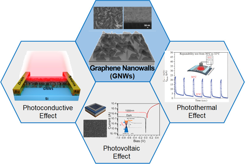
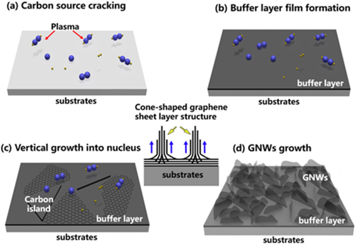
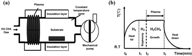
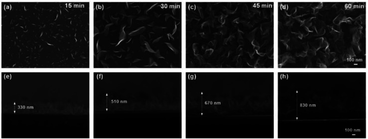
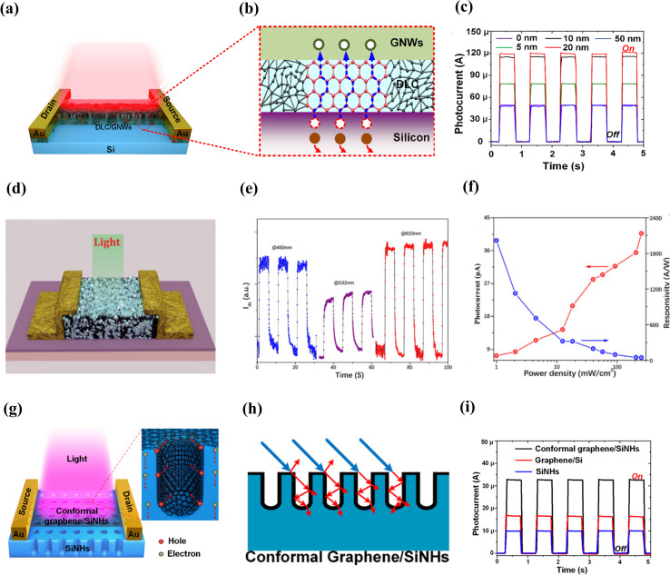
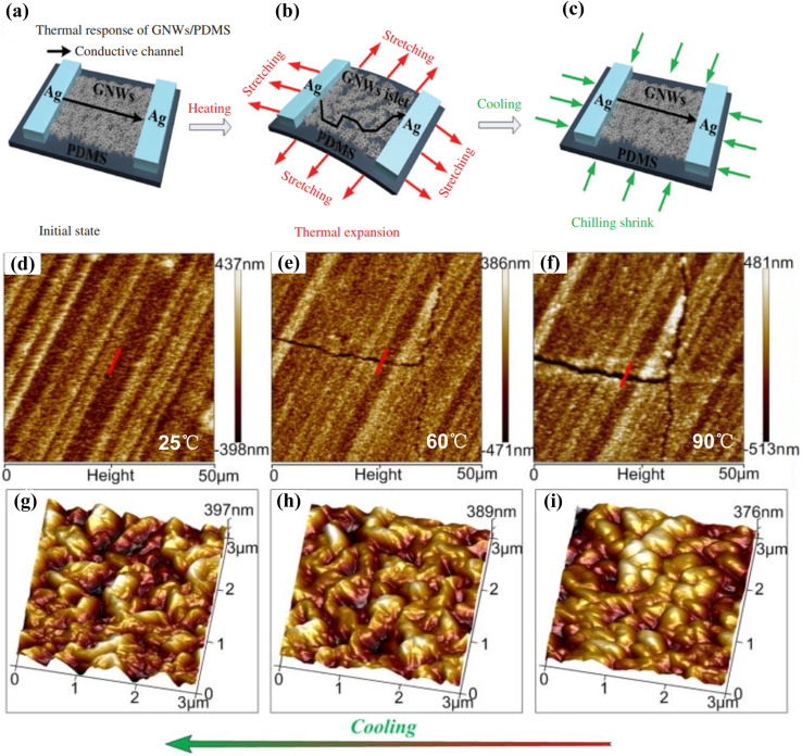
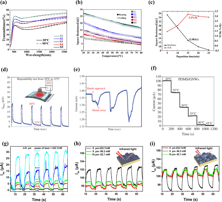
Graphene nanowalls (GNWs) have emerged as a promising material in the field of photodetection, thanks to their exceptional optical, electrical, mechanical, and thermodynamic properties. However, the lack of a comprehensive review in this domain hinders the understanding of GNWs' development and potential applications. This review aims to provide a systematic summary and analysis of the current research status and challenges in GNW-based photodetectors. We begin by outlining the growth mechanisms and methods of GNWs, followed by a discussion on their physical properties. Next, we categorize and analyze the latest research progress in GNW photodetectors, focusing on photovoltaic, photoconductive, and photothermal detectors. Lastly, we offer a summary and outlook, identifying potential challenges and outlining industry development directions. This review serves as a valuable reference for researchers and industry professionals in understanding and exploring the opportunities of GNW materials in photodetection.


Conflict of interest statement

The authors declare that they have no known competing financial interests or personal relationships that could have appeared to influence the work reported in this paper.

Figures

Fig. 1
Fig. 1. Photodetectors based on GNWs. Copyright © 2021, American Chemical Society. Copyright © 2017, Royal Society of Chemistry. Copyright © 2018, De Gruyter.
Fig. 2
Fig. 2. Growth mechanism of GNWs. (a) Dissociation of carbon–hydrogen bonds by plasma; (b) formation of the buffer layer; (c) nucleation of vertical graphene; (d) growth of GNWs.
Fig. 3
Fig. 3. Growth process of GMWs. (a) Schematic diagram of RF-PECVD equipment for the growth of GNWs. (b) Schematic illustrating the preparation process of GNWs.
Fig. 4
Fig. 4. SEM images of GNWs with different growth time. (a)–(d) Top-view images; (e)–(h) cross-sectional images.
Fig. 5
Fig. 5. TEM images and Raman spectra of GNWs. (a) Low magnification; (b) high magnification. (c) SAED pattern of the area indicated by white circle in MLG nanowalls; Copy right © 2012, Elsevier Ltd. (d) Raman spectra of GNWs and graphene film; Raman spectrum of MLG nanowalls grown for 60 min excited by (e) 633 nm and (f) 514 nm lasers. Copy right © 2012, Elsevier Ltd.
Fig. 6
Fig. 6. Absorption spectra of GNWs with different growth time. (a) Transmittance; (b) absorbancy; (c) optoelectronic properties of the DLC interlayer with different thicknesses before and after annealing. Copyright © 2021, American Chemical Society.
Fig. 7
Fig. 7. Sheet resistance (a) and conductivity (b) of GNWs; (c) plots of absorption curves calculated from the Tauc method for DLC film with different thicknesses; (d) band gap of DLC films with different thicknesses with and without annealing; Copyright © 2021, American Chemical Society. (e) The conductivity of a GNWs/Si and a GNWs/UVA hybrid film. © 2022 Elsevier B.V. All rights reserved. (f) Nyquist plots of EIS spectra recorded for the GWs and CdS-GWs (160 cycles) electrodes under the visible-light illumination (100 mW cm−2), in the electrolyte of 0.1 M Na2S. Copyright © 2015 Elsevier B.V.
Fig. 8
Fig. 8. Interface adhesion between GNWs and silicon substrate. (a) Cross-sectional SEM image of Si/GNWs; (b) micropattern of Si/GNWs. (c) and (d) high-magnification cross-sectional TEM images of Si/DLC/GNWs. Copyright © 2021, American Chemical Society.
Fig. 9
Fig. 9. Energy band structure of GNWs/Si. (a) Uncontacted; (b) contacted; (c) schematic diagram of energy band structure of GNWs/Si heterojunction. Copyright © 2019, American Chemical Society.
Fig. 10
Fig. 10. GNWs-based photovoltaic detectors. (a) Schematic representation of the GNWs/Si heterojunction detector structure; (b) illustration of the energy band diagram of the device; (c) device response under 8–14 μm laser excitation; (d) photocurrent response of the device at varying optical power levels; (e) response time characteristics of the device; (f) noise current associated with the device. Copyright © 2017, Royal Society of Chemistry.
Fig. 11
Fig. 11. GNWs-based photovoltaic detectors. (a) Schematic illustration of the GNW heterostructure device grown on Si via PECVD; (b and c) device response at different wavelength bands; Copyright © 2019, AIP Publishing (d) schematic representation of the Si/Au/GNWs heterojunction device, incorporating Au nanoparticles on Si before the PECVD growth of GNWs; (e) variation in the device's absorption rate before and after the addition of Au; (f)–(i) photoresponse performance of the Si/Au/GNWs heterojunction detector. Copyright © 2019, American Chemical Society.
Fig. 12
Fig. 12. GNWs-based photovoltaic detectors (a) fabrication process of GNWs using the PEALD method; (b) schematic illustration of the device structure; (c)–(f) photoelectric detection performance of the device; Copyright © 2021, American Chemical Society (g) schematic representation of the 3D-Gr/2D-Gr/Ge heterojunction detector structure; (h) photoelectric response currents of the 3D-Gr/2D-Gr/Ge heterojunction detector at various 1550 nm light power levels; (i) response time of the 3D-Gr/2D-Gr/Ge heterojunction detector. Copyright © 2020, American Chemical Society.
Fig. 13
Fig. 13. Photogating effect of low dimensional materials. (a) Photocarriers in the photosensitive layer entering the conductive channel; (b) photocarriers in the photosensitive layer gathering at the interface; (c) influence of source–drain bias voltage on photocurrent; (d) influence of gate voltage on photocurrent.
Fig. 14
Fig. 14. Photogating effect of GNWs/semiconductor heterojunction. (a) Dark current under an external bias due to intrinsic carriers in GNWs; (b) incident photons generate electron–hole pairs in the silicon; (c) these injected carriers gate the GNWs channel; (d) at the end of their lifetime, these carriers recombine back into silicon.
Fig. 15
Fig. 15. GNWs-based photoconductive detectors. (a) and (b) Schematic diagram of optoelectronic detector device structures using GNWs on different Si substrates; (c) photoresponse of the three devices; Copyright © 2020 Elsevier Ltd. All rights reserved. (d) Schematic diagram of the VOG/Ge heterojunction photodetector. (e) UV-NIR absorption spectra of VOG/Ge and GQDs/VOG/Ge. (f) Photoresponse properties of the GQDs/VOG/Ge device under irradiation with light of 1550 nm with variable light intensities. The applied bias is 1 V. Copyright © 2020, American Chemical Society.
Fig. 16
Fig. 16. GNWs-based photoconductive detectors. (a) and (b) Device structure and energy band diagram of photoconductive devices prepared by growing GNWs on SnO2 film; (c) photoresponse performance of SnO2/GNWs devices; Copyright © 2018 Elsevier B.V. (d) Schematic diagram of FET device structure directly grown GNWs on SnO2 insulating layer substrate using PECVD; (e) photocurrent (Iph) of the GNWs photodetector at various gate voltages; (f) time-dependent Iph measurements of the GNWs photodetector and MLG photodetector working at their respective Dirac point voltage under the illumination of a 1550 nm laser, VSD = 100 mV. Reprinted with permission from Copyright © The Optical Society.
Fig. 17
Fig. 17. GNWs-based photoconductive detectors. (a) Schematic representation of Si/DLC/GNWs heterostructure device; (b) transformation of DLC layer to graphene-like structure after annealing; (c) infrared detection capability of Si/DLC/GNWs heterostructure device; Copyright © 2021, American Chemical Society. (d) Schematic of perovskite/GNWs photodetector device; (e) and (f) photoresponse performance of perovskite/GNWs photodetector device. Image source: “Lateral Structured Phototransistor Based on Mesoscopic Graphene/Perovskite Heterojunctions” (https://www.mdpi.com/2079-4991/11/3/641) by [Dahua Zhou*, Leyong Yu, Peng Zhu, Hongquan Zhao, Shuanglong Feng and Jun Shen] published under the Creative Commons Attribution License (CC BY) by MDPI. (g) Schematic view of the conformal graphene/SiNHs detectors. (h) Schematic view of the conformal graphene/SiNHs (i) measured photoresponse of the planar graphene/Si, SiNHs, and conformal graphene/SiNH detectors. Copyright © 2019, American Chemical Society.
Fig. 18
Fig. 18. GNWs-based photothermal detector. (a)–(c) Schematic diagram of the thermal response of GNWs/PDMS composites. Copyright © 2018, De Gruyter (d)–(f) surface morphology change of GNWs film under different temperature from 25 to 90 °C. AFM image of cracks evolution on GNWs film (50 × 50 μm) (g)–(i) the AFM cross-section of crack region (3 μm). Copyright © 2011, RSC Publishing.
Fig. 19
Fig. 19. GNWs-based photothermal detector. (a) Emissivity of GNWs/VO2 devices at different GNWs deposition times (S1 = 5 min, S2 = 10 min, S3 = 15 min, S4 = 20 min, S5 = 25 min); (b) sheet resistance values of devices at different GNWs deposition times; (c) TCR and sheet resistance of optimized thickness device; Copyright © 2020 The Chinese Ceramic Society. Production and hosting by Elsevier B.V. (d)–(f) Photoresponse properties of photodetectors based on GNWs/PDMS composites; Copyright © 2018, De Gruyter. (g) The photocurrent of the GNWs/UVA detector underdifferent bias voltages at the wavelength of 8 μm at room temperature; (h) the photocurrent of the GNWs/UVA detector under different wavelengths from 8–10 μm before dripping; (i) the photocurrents of the GNWs/UVA detector under different wavelengths from 8–10 μm after dripping. Copyright © 2022 Elsevier B.V. All rights reserved.

Similar articles

Cited by

References

    1. Hou F. et al., Review on Infrared Imaging Technology. Sustainability. 2022;14(18):11161.
    1. Hu X. et al., Recent developments of infrared photodetectors with low-dimensional inorganic nanostructures. Nano Res. 2022;15(2):805–817.
    1. Hu W.-D. et al., Recent progress on advanced infrared photodetectors. Acta Phys. Sin. 2019;68(12):120701.
    1. Liu J. et al., Development of long-wavelength infrared detector and its space-based application requirements. Chin. Phys. B. 2019;28(2):028504.
    1. Lu X. et al., Progress of Photodetectors Based on the Photothermoelectric Effect. Adv. Mater. 2019;31(50):1902044. - PubMed