Review
. 2023 Aug 23;123(16):9982-10078.
doi: 10.1021/acs.chemrev.3c00139. Epub 2023 Aug 5.

Transparent Electronics for Wearable Electronics Application

Affiliations
Review

Transparent Electronics for Wearable Electronics Application

Daeyeon Won et al. Chem Rev. .

Abstract

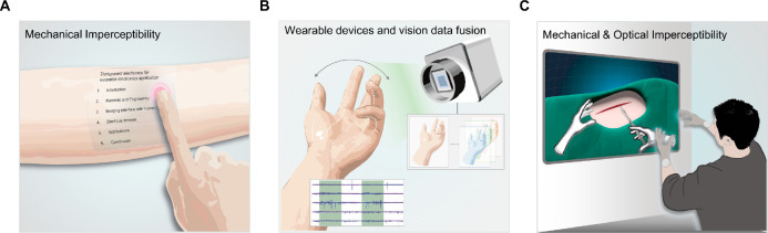
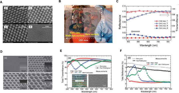
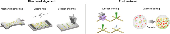
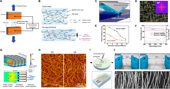
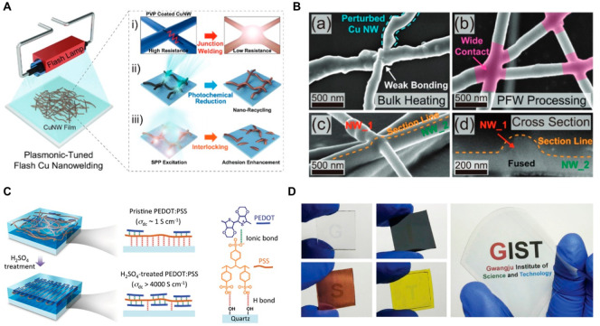
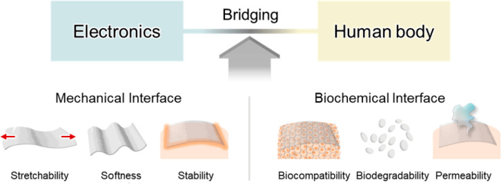
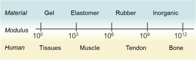
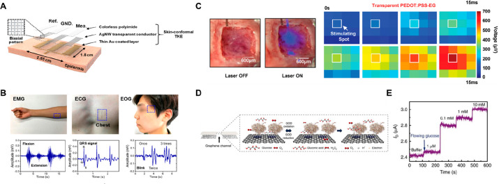
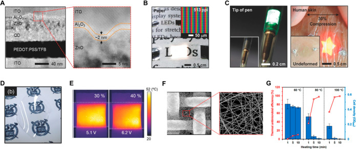
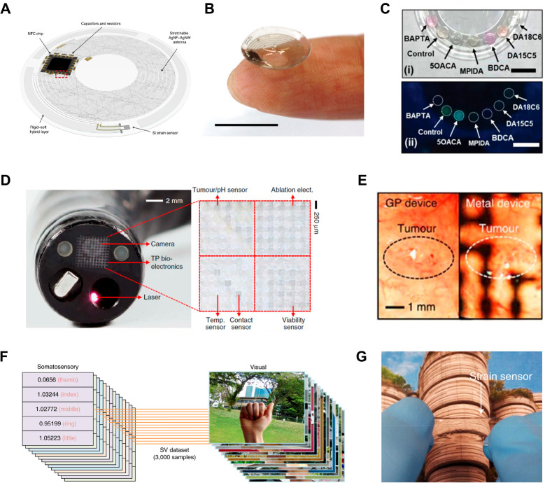
Recent advancements in wearable electronics offer seamless integration with the human body for extracting various biophysical and biochemical information for real-time health monitoring, clinical diagnostics, and augmented reality. Enormous efforts have been dedicated to imparting stretchability/flexibility and softness to electronic devices through materials science and structural modifications that enable stable and comfortable integration of these devices with the curvilinear and soft human body. However, the optical properties of these devices are still in the early stages of consideration. By incorporating transparency, visual information from interfacing biological systems can be preserved and utilized for comprehensive clinical diagnosis with image analysis techniques. Additionally, transparency provides optical imperceptibility, alleviating reluctance to wear the device on exposed skin. This review discusses the recent advancement of transparent wearable electronics in a comprehensive way that includes materials, processing, devices, and applications. Materials for transparent wearable electronics are discussed regarding their characteristics, synthesis, and engineering strategies for property enhancements. We also examine bridging techniques for stable integration with the soft human body. Building blocks for wearable electronic systems, including sensors, energy devices, actuators, and displays, are discussed with their mechanisms and performances. Lastly, we summarize the potential applications and conclude with the remaining challenges and prospects.


Conflict of interest statement

The authors declare no competing financial interest.

Figures

Figure 1
Figure 1
The mechanical and optical imperceptibility of wearable electronics. The mechanical imperceptibility of wearable devices for skin-conformal integration. (B) Optical imperceptibility for the fusion of vision data and wearable electronics. (C) The mechanical and optical imperceptibility of wearable electronics for efficient XR applications.
Figure 2
Figure 2
Thin film growth modes. (A) Schematic illustration of thin film growth modes. Depending on the interaction between the metal atom, the adjacent atom, and the substrate, three different mechanisms occur over time: Volmer–Weber mode (island growth), Stranski–Krastanov mode (layer + island growth), and Frank–van der Merwe mode (layer by layer mode). (B) Scanning electron microscopy images representing different morphologies of Ag thin films with thicknesses of 1, 4.5, 7.2, and 12.6 nm. Scale bar, 500 nm. Reproduced with permission from ref (62). Copyright 2017 Springer Nature under the CC BY 4.0 license http://creativecommons.org/licenses/by/4.0/.
Figure 3
Figure 3
Metal nanomaterials. (A) Graphical illustration of chemical reduction method for synthesizing metal nanomaterials. Representative SEM images of (B) AuNPs. Reproduced from ref (92). Copyright 2016 American Chemical Society. (C) AgNPs. Reproduced with permission from ref (97). Copyright 2009 Elsevier. (D) AgNWs. Reproduced from ref (129). Copyright 2012 American Chemical Society. (E) CuNWs. Reproduced from ref (137). Copyright 2005 American Chemical Society.
Figure 4
Figure 4
Synthesis of graphene. (A) Major fabrication methods of graphene. Top-down methods include mechanical cleavage and liquid-phase exfoliation of graphite. Additionally, the chemical exfoliation of graphite produces GO, which is then reduced to rGO. CVD is a representative bottom-up method that involves the decomposition of carbon sources and the subsequent deposition of carbon atoms onto substrates. (B) Photograph of a multilayer graphene flake fabricated by micromechanical cleavage. Reproduced with permission from ref (34). Copyright 2004 American Association for the Advancement of Science. (C) TEM images of a typical monolayer graphene flake fabricated by the liquid-phase exfoliation method. Inset: a diffraction pattern taken from a monolayer. Reproduced with permission from ref (165). Copyright 2010 Wiley-VCH. (D) SEM image of rGO flakes on Si/SiO2 substrate. Reproduced with permission from ref (178). Copyright 2013 Wiley-VCH. (E) SEM images of graphene on Cu grown by CVD. Reproduced from ref (185). Copyright 2011 American Chemical Society.
Figure 5
Figure 5
Conducting polymers. (A) Log-scale conductivity charts that compare the conductivity range of conjugated polymers to metallic conductors, semiconductors, and insulators. (B) Chemical structures of representative conducting polymers.
Figure 6
Figure 6
Metal oxides. (A) Schematic orbital diagrams representing the carrier transport pathways in crystalline and amorphous metal oxides. (B) Band alignment of the representative metal oxides. Reproduced with permission from ref (328). Copyright 2011 IOP Publishing Ltd.
Figure 7
Figure 7
Metal oxide-based transparent and flexible sensors. (A) SEM image of ZnO nanoparticle. (B,C) Optical images showing transparency and flexibility of PET-ITO-ZnO device. (D) The gas sensing performance of the device under 370 nm light illuminations (5 mW) at room temperature. Reproduced with permission from ref (350). Copyright 2015 Springer Nature under the CC BY 4.0 license http://creativecommons.org/licenses/by/4.0/. (E) SEM image of In2O3 nanowires. (F) Transparent and flexible gas sensor based on In2O3 nanowires. (G) Sensor response depending on NO2 concentrations under blue LED illumination. Reproduced with permission from ref (300). Copyright 2012 Royal Society of Chemistry.
Figure 8
Figure 8
TMDCs. (A) Schematics of the 3D structure of TMDCs with the common formula MX2. (B) Optical micrographs of MoS2 ultrathin crystals fabricated by modified micromechanical cleavage. Reproduced with permission from ref (397), Copyright 2010 AIP Publishing. (C) Optical microscope (left) and SEM (right) images of an electrochemically exfoliated monolayer MoS2 nanosheet deposited on SiO2 substrate. Reproduced from ref (305). Copyright 2014 American Chemical Society. (D) AFM image of the MoS2 grown by CVD. The height scale bar is 20 nm. Reproduced with permission from ref (306). Copyright 2016 Wiley-VCH. (E) Photograph of transparent and flexible MoS2 transistor arrays on the human wrist. Inset: the magnified image of FET arrays. Reproduced with permission from ref (308). Copyright 2020 Springer Nature.
Figure 9
Figure 9
Chemical structures for a range of commonly used small-molecule and semiconducting polymers.
Figure 10
Figure 10
The optical and electrical properties of transparent electronics. (A) Trade-off relationship of optical and electrical properties. (B) Concepts to secure transparency of electronic devices.
Figure 11
Figure 11
Random percolation networks. (A) Schematic illustration of transparent electronics enabled by random percolation networks of electronic materials. (B) SEM image of spin-coated AgNW random percolation networks depending on spin rates. Reproduced with permission from ref (493). Copyright 2013 Wiley-VCH. (C) Optical image of a spray-coated large area of rGO sheet. (D) The transmittance of a large area of rGO with over 80% in the visible range. Reproduced with permission from ref (286). Copyright 2014 Wiley-VCH. (E) Optical image of vacuum filtration transferred transparent AgNW conductor on PDMS substrate. (F) The transmittance of AgNW transparent conductor by varying the density of random percolation networks. Reproduced with permission from ref (153). Copyright 2015 Wiley-VCH. (G) Schematic illustration of electrospinning-based random percolation networks transparent conductor. (H) Optical images of electro-spun transparent conductors on various substrates. Reproduced with permission from ref (499). Copyright 2013 Springer Nature.
Figure 12
Figure 12
Grid patterning. (A) Schematic illustration of nanoimprinting technique to fabricate AuNW-based transparent conductor. (B) SEM image of grid-patterned AuNW transparent conductor. Reproduced from ref (501). Copyright 2016 American Chemical Society. (C,D) Schematic illustration of optical microlithography for patterning organic semiconductors, conductors, and dielectrics. (E) Optical images of fabricated 42 000 transistors consist of patterned organic materials in a small area. Reproduced with permission from ref (551). Copyright 2021 American Association for the Advancement of Science. (F,G) Schematic illustration of direct laser sintering process to fabricate grid patterned Ag transparent conductor. (H) Optical image and SEM image of grid-patterned transparent Ag conductors. Reproduced with permission from ref (506). Copyright 2019 Springer Nature under the CC BY 4.0 license http://creativecommons.org/licenses/by/4.0/. (I) Schematic illustration of inkjet printing of AgNP inks for grid-patterned transparent conductors. (J,K) Optical images of grid-patterned transparent conductors. Reproduced with permission from ref (508). Copyright 2015 Wiley-VCH.
Figure 13
Figure 13
Subwavelength structure. (A) SEM images of the subwavelength structure referred to as the moth-eye structure. Reproduced with permission from ref (564). Copyright 2010 Wiley-VCH. (B) Digital image of bare glass and SWS structured glass showing a clear difference in reflectivity. (C) Reflectance and transmittance of SWS structure depending on process condition. Reproduced with permission from ref (565). Copyright 2009 Royal Society of Chemistry. (D) SEM images of inverted moth-eye structure in PDMS sheet. (E) Total transmittance of bare PDMS and SWS PDMS. (F) Total transmittance of bare PDMS and SWS PDMS. Reproduced with permission from ref (566). Copyright 2014 Wiley-VCH.
Figure 14
Figure 14
Engineering strategies to enhance electrical properties of transparent electrodes and active materials.
Figure 15
Figure 15
Directional alignment. (A) Schematic illustration of mechanical stretching of PEDOT:PSS for rearrangement of polymer chain structures. Reproduced with permission from ref (510). Copyright 2013 Wiley-VCH. (B) Schematic illustration of polymer chains under mechanical deformation. Reproduced with permission from ref (573). Copyright 2016 Springer Nature under the CC BY 4.0 license http://creativecommons.org/licenses/by/4.0/. (C) Schematic illustration of solution shearing of AgNW solution to directional alignment. (D) SEM image of aligned AgNWs. (E) The sheet resistance of aligned AgNW showing higher conductivity than random percolated AgNW. (F) The transmittance of aligned AgNW-based transparent conductor and random percolated conductor. Reproduced from ref (512). Copyright 2015 American Chemical Society. (G) Schematic illustration of solution shearing of organic semiconductors using the micropatterned channel. (H) AFM images of aligned organic semiconductors and spin-coated counterparts. Reproduced with permission from ref (575). Copyright 2019 Springer Nature. (I) Schematic illustration of floating assembly to align and pack AgNW networks using surfactant dropping. (J) Optical images of aligned AgNW conductors showing high stretchability. Reproduced with permission from ref (515). Copyright 2021 American Association for the Advancement of Science.
Figure 16
Figure 16
Post-treatments. (A) Schematic illustration of photothermal annealing induced nanowire welding process. (B) SEM images of photothermally welded CuNW percolation networks. Reproduced with permission from ref (516). Copyright 2017 Wiley-VCH. (C) Schematic illustration of post-treatment of PEDOT:PSS in H2SO4 for conductivity enhancement. (D) Optical images of PEDOT:PSS after cleaning H2SO4 and transferring on the various substrate. Reproduced with permission from ref (519). Copyright 2015 Wiley-VCH.
Figure 17
Figure 17
Bridging interface with the human body.
Figure 18
Figure 18
Elastic modulus of various electronic materials and biological tissues.
Figure 19
Figure 19
Structural engineering. (A) Schematic illustration of the ultrathin thickness of the stretchable elastic conductor. (B,C) Optical images of stretchable ultrathin electronics interfacing with human skin and rat nerves. Reproduced with permission from ref (593). Copyright 2022 Springer Nature. (D) Schematic illustration of prestrain methods for high stretchability. (E) SEM image of wrinkled AgNW percolation networks. (F) Optical image of the large area of prestrained AgNW transparent conductor. (G) The transmittance of prestrained AgNW percolation networks. Reproduced with permission from ref (595). Copyright 2020 Wiley-VCH. (H,I) Optical images of stretchable serpentine graphene electronics. (J) IV curves of μLED under various strains. Reproduced from ref (6). Copyright 2011 American Chemical Society. (K) Schematic illustration of stretchable Kirigami conductor. (L) Change in resistance of Kirigami conductor under cyclic mechanical deformation. (M) Optical image of conformal contact of Kirigami conductor on human skin. Reproduced from ref (599). Copyright 2019 American Chemical Society.
Figure 20
Figure 20
Materials engineering. (A) Schematic illustration of supramolecular chain engineering for high stretchability of PEDOT:PSS. (B) Optical images of stretchable transparent PEDOT:PSS under tensile strain. (C) Conformal contact of stretchable PEDOT conductor on the mouse brain. Reproduced with permission from ref (603). Copyright 2022 American Association for the Advancement of Science. (D) Schematic illustration of stretchable organic semiconductor fabricated by nanoconfinement effect. (E) Optical image of organic semiconductor films under tensile strain. (F),(G) Optical image of the high transparency of organic semiconductors and conformal contact to human skin. Reproduced with permission from ref (10). Copyright 2017 American Association for the Advancement of Science.
Figure 21
Figure 21
Conductive elastomer. (A) Schematic illustration of surface-initiated atom transfer radical polymerization with liquid metal and various polymer matrices. (B) Optical image of transparent liquid metal-based conductive elastomer. (C,D) High stretchability of liquid metal-based conductive elastomer. Reproduced with permission from ref (605). Copyright 2019 Springer Nature. (E) Molecular structure of transparent ionic conductive elastomer. (F) Optical image of highly transparent ionic conductive elastomer. (G) Stress–strain curve of transparent conductive elastomer. (H) Strong adhesion of ionic conductive elastomer to various substrates. Reproduced with permission from ref (606). Copyright 2018 Springer Nature under the CC BY 4.0 license http://creativecommons.org/licenses/by/4.0/.
Figure 22
Figure 22
Conductive hydrogels. (A) Schematic illustration of interpenetrating networks of conductive hydrogels using PEDOT:PSS and PAA networks. (B) Optical image of conductive hydrogels under 250% of tensile strain. (C) Stress–strain curves of conductive hydrogels varying compositions of PEDOT:PSS and PAA contents. Reproduced with permission from ref (609). Copyright 2018 Springer Nature under the CC BY 4.0 license http://creativecommons.org/licenses/by/4.0/. (D) Schematic illustration of highly tough and stretchable conductive hydrogels by orthogonal photochemical reactions. (E) Optical images of highly tough and stretchable conductive hydrogels. (F) Stress–strain curve of conductive hydrogels. Reproduced with permission from ref (653). Copyright 2021 Springer Nature under the CC BY 4.0 license http://creativecommons.org/licenses/by/4.0/.
Figure 23
Figure 23
Long-term stability. (A) Schematic illustration of high adhesion of graphene-based adhesive layer on biological tissues. (B) The adhesive layer enabled the stable operation of bioelectronic devices on the heart. Reproduced with permission from ref (658). Copyright 2020 Springer Nature. (C) Schematic illustration of a gas and mass permeable conductor using nanofiber networks and AgNW. (D), (E) Optical images of transparent permeable conductors and stable contact with human skin. (F) Air permeability of the assembled conductor. Reproduced from ref (667). Copyright 2018 American Chemical Society. (G) Schematic illustration of self-healable CNT electronics. (H) Optical image of the healing process of stretchable CNT electronics. Reproduced with permission from ref (679). Copyright 2018 Springer Nature.
Figure 24
Figure 24
Biocompatibility. (A) Optical image of silk used for stretchable and biocompatible substrates. (B) SEM image of AgNW percolation networks on silk substrate. (C) Transmittance of silk-based AgNW conductor. Reproduced from ref (687). Copyright 2014 American Chemical Society. (D) Schematic illustration of PEGDE-reinforced silk-based electronics. (E) Transmittance of PEGDE and silk conductors. (F) Optical image of stable contact of silk electronics on the mouse brain. Reproduced with permission from ref (688). Copyright 2021 Wiley-VCH. (G) Schematic illustration of core–shell nanowire synthesis. (H) TEM image of synthesized Ag–Au core–shell nanowire. (I) Optical image of core–shell nanowire under corrosive environment. Reproduced from ref (695). Copyright 2016 American Chemical Society. (J) Schematic illustration and SEM image of Ag–Au–PPy core–shell nanowires. (K) TEM image of Ag–Au–Ppy core–shell nanowire. (L) Optical image of transparent core–shell nanowires. Reproduced with permission from ref (697). Copyright 2017 Springer Nature under the CC BY 4.0 license http://creativecommons.org/licenses/by/4.0/.
Figure 25
Figure 25
Biodegradability. (A) Optical image of biodegradable and transparent optical fiber fabricated by PLLA. (B) SEM image of transparent PLLA fiber. (C) Transmittance of PLLA optical fibers. (D) Biodegradation of PLLA fiber in water. Reproduced with permission from ref (700). Copyright 2017 Wiley-VCH. (E) Optical image of biodegradable and transparent conductors. (F) The transmittance of biodegradable conductors varying thicknesses. (G,H) SEM images of biodegraded electronics for 6 days. Reproduced with permission from ref (701). Copyright 2019 Wiley-VCH. (I) Schematic illustration of actively triggered biodegradable electronics using ultrasound. (J) Optical images of degraded electronics by ultrasound. (K) The output voltage of energy device under different power of ultrasound. Reproduced with permission from ref (710). Copyright 2022 American Association for the Advancement of Science under the CC BY-NC 4.0 license https://creativecommons.org/licenses/by-nc/4.0/.
Figure 26
Figure 26
Thermal protection layer. (A) SEM cross-sectional image porous aerogel fiber that have graded structures inside. (B) The temperature response to the thermal protection layer. Reproduced from ref (713). Copyright 2022 American Chemical Society. (C) Schematic illustration of PCM microsphere embedded PDMS composite (D) Digital image of highly stretchable thermal protection layer. (E) Thermal images of mouse skin under normal PDMS and thermal protection layer after heating. Reproduced with permission from ref (716). Copyright 2022 Springer Nature under the CC BY 4.0 license http://creativecommons.org/licenses/by/4.0/.
Figure 27
Figure 27
Heat dissipation layer. (A) Schematic illustration of heat conduction composite with PVA and BN nanosheet. (B) Aligned BN nanosheet in composite fiber. (C) Digital image of heat conductive fiber in textiles. Reproduced from ref (717). Copyright 2017 American Chemical Society. (D) Schematic illustration of the visibly transparent radiative cooler. (E) SEM images of multilayers of the radiative cooler. (F) Digital image of the transparent radiative cooler. (G) IR camera image measured outdoors. Reproduced with permission from ref (719). Copyright 2021 Wiley-VCH.
Figure 28
Figure 28
Physical sensors. (A) Optical image of a free-standing transparent electrode. (B) The variation in the electrical current by the different surface morphologies Reproduced with permission from ref (506). Copyright 2019 Springer Nature. (C) The change in the resistance of an L4S90 hydrogel before and after self-healing. (D) The relationship between the resistance ratio and strain. Reproduced from ref (724). Copyright 2019 American Chemical Society. (E) Thin, transparent iontronic film on the electrode substrate. (F) The capacitive values measured from the device when subjected to repetitive cycles of external pressure, exceeding 30 000 cycles. Reproduced with permission from ref (726). Copyright 2015 Wiley-VCH. (G) The transparent piezoelectric motion sensor conforming to the contours of a human wrist. (H) The voltage output of sensors with PLA and SWNT-embedded PLA. Reproduced with permission from ref (591). Copyright 2014 Wiley-VCH. (I) Optical image of micropatterned PDMS triboelectric sensor. (J) The output voltage of a PDMS thin film sensor with different micropatterns. Reproduced from ref (731). Copyright 2012 American Chemical Society. (K) Optical images of a stretchable and conformable gated temperature sensor. (L) A comparison of the temperature responses of a gated sensor and a resistor sensor. Reproduced with permission from ref (733). Copyright 2015 Wiley-VCH.
Figure 29
Figure 29
Physiological sensors. (A) Schematic illustration of transparent Kirigami electrophysiological sensor. (B) Capturing various electrophysiology signals (EMG, ECG, and EOG). Reproduced from ref (599). Copyright 2019 American Chemical Society. (C) Optical images and electrophysiological mapping of the PEDOT:PSS-EG electrode applied by a blue laser. Reproduced with permission from ref (739). Copyright 2021 Wiley-VCH under the CC BY-NC 4.0 license https://creativecommons.org/licenses/by-nc/4.0/. (D) Schematic illustration of glucose detection. (E) The current values at the glucose concentration from 1 mM to 10 mM. Reproduced with permission from ref (460). Copyright 2017 Springer Nature under the CC BY 4.0 license http://creativecommons.org/licenses/by/4.0/.
Figure 30
Figure 30
Energy storages. (A) A series-connected supercapacitor. (B) The areal capacitance of Ag/Au, Ag/Au/ppy supercapacitor as a function of the current density. Reproduced with permission from ref (697). Copyright 2017 Springer Nature under the CC BY 4.0 license http://creativecommons.org/licenses/by/4.0/. (C) Areal capacitance at various current densities and photographs of SWCNT film and the asymmetric device. (D) Galvanostatic charge–discharge at different current densities of the asymmetric device. Reproduced with permission from ref (800). Copyright 2017 Wiley-VCH. (E) Optical image and SEM image of a transparent and flexible battery electrode. (F) The optical transparency versus energy density. (10Wh/L at 60% transmittance) Reproduced with permission from ref (805). Copyright 2011 National Academy of Sciences. (G) Image of an FE-ZiB device in the (left) charged state at 1.6 V and (right) discharged state at 0.3 V. (H) Areal capacity under various area current densities. Reproduced with permission from ref (807). Copyright 2021 Wiley-VCH.
Figure 31
Figure 31
Energy harvesters. (A) SEM image of the AgNWs embedded into the PET film. (B) The open-circuit voltage during repeated bending and unbending. Reproduced with permission from ref (586). Copyright 2016 Wiley-VCH. (C) Digital images of a different stretched state of triboelectric nanogenerator. (D) The output voltage of triboelectric nanogenerator. Reproduced with permission from ref (814). Copyright 2017 American Association for the Advancement of Science under the CC BY-NC 4.0 license https://creativecommons.org/licenses/by-nc/4.0/. (E) A CuI thin film on PET. (F) Output voltage and output power of a CuI-based thermoelectric energy harvester. Reproduced with permission from ref (818). Copyright 2017 Springer Nature under the CC BY 4.0 license http://creativecommons.org/licenses/by/4.0/. (G) Schematic illustration of wireless power devices. (H) Inductance variation versus frequency of various multiturn spiral coils. Reproduced with permission from ref (843). Copyright 2020 Springer Nature under the CC BY 4.0 license http://creativecommons.org/licenses/by/4.0/.
Figure 32
Figure 32
Actuators. Various applications of hydrogel actuators and robots. (A) Forward fish-like swimming robotic fish. (B) A hydrogel actuator kicking a rubber-ball in water. (C) A hydrogel gripper. Reproduced with permission from ref (855). Copyright 2017 Springer Nature under the CC BY 4.0 license http://creativecommons.org/licenses/by/4.0/. (D) A Peano-HASEL actuator and the submerged portion of the actuator are nearly invisible. (E) Submerged actuator lifting 10 g weight under 8 kV. Reproduced with permission from ref (859). Copyright 2018 American Association for the Advancement of Science. (F) An LCE artificial muscle film lifting an object of 400 g. Reproduced with permission from ref (865). Copyright 2019 American Association for the Advancement of Science under the CC BY-NC 4.0 license https://creativecommons.org/licenses/by-nc/4.0/.
Figure 33
Figure 33
Display, heater, air filter. (A) Cross-sectional scanning TEM image of the Tr-QLED. (B) The array is patterned by the intaglio transfer printing method (513 pixels in–1). (C) Digital image of transparent flexible Tr-QLED. Reproduced with permission from ref (797). Copyright 2017 Wiley-VCH. (D) Digital image of AgNWs transparent stretchable heater. (E) Temperature distribution under various strains with adjusted voltage to maintain constant temperatures (50 °C). Reproduced with permission from ref (153). Copyright 2015 Wiley-VCH. (F) SEM images of CuNWs on nylon mesh. (G) Bacterial growth and corresponding thermal antimicrobial efficiencies. Reproduced from ref (912). Copyright 2022 American Chemical Society.
Figure 34
Figure 34
Various wearable electronics applications.
Figure 35
Figure 35
Transparent wearable electronics applications. (A) Schematic illustration of an integrated system including strain sensor, antenna, NFC chip, and interconnects. (B) Digital image of smart contact lens. Reproduced with permission from ref (919). Copyright 2021 Springer Nature. (C) Digital image of multiplexed scleral lens with fluorescent probes. Reproduced with permission from ref (920). Copyright 2019 Wiley-VCH under the CC BY 4.0 license http://creativecommons.org/licenses/by/4.0/. (D) Digital image of a multifunctional endoscope system. (E) Digital image of tumor captured by transparent bioelectronic devices, and control metal devices. Reproduced with permission from ref (922). Copyright 2015 Springer Nature under the CC BY 4.0 license http://creativecommons.org/licenses/by/4.0/. (F) Illustration of the data sets for multimodal fusion. (G) Digital image of stretchable transparent strain sensor. Reproduced with permission from ref (720). Copyright 2020 Springer Nature.
Figure 36
Figure 36
Challenges of transparent wearable electronics.

References

    1. Ray T. R.; Choi J.; Bandodkar A. J.; Krishnan S.; Gutruf P.; Tian L.; Ghaffari R.; Rogers J. A. Bio-Integrated Wearable Systems: A Comprehensive Review. Chem. Rev. 2019, 119, 5461–5533. 10.1021/acs.chemrev.8b00573. - DOI - PubMed
    1. Ates H. C.; Nguyen P. Q.; Gonzalez-Macia L.; Morales-Narvaez E.; Guder F.; Collins J. J.; Dincer C. End-to-end design of wearable sensors. Nat. Rev. Mater. 2022, 7, 887–907. 10.1038/s41578-022-00460-x. - DOI - PMC - PubMed
    1. Pyun K. R.; Rogers J. A.; Ko S. H. Materials and devices for immersive virtual reality. Nat. Rev. Mater. 2022, 7, 841–843. 10.1038/s41578-022-00501-5. - DOI - PMC - PubMed
    1. Feiner R.; Dvir T. Tissue-electronics interfaces: from implantable devices to engineered tissues. Nat. Rev. Mater. 2018, 3, 17076.10.1038/natrevmats.2017.76. - DOI
    1. Webb R. C.; Bonifas A. P.; Behnaz A.; Zhang Y.; Yu K. J.; Cheng H.; Shi M.; Bian Z.; Liu Z.; Kim Y. S.; et al. Ultrathin conformal devices for precise and continuous thermal characterization of human skin. Nat. Mater. 2013, 12, 938–944. 10.1038/nmat3755. - DOI - PMC - PubMed

Publication types

LinkOut - more resources