

Fabrication of Silicon Nanowires by Metal-Assisted Chemical Etching Combined with Micro-Vibration
- PMID: 37570187
- PMCID: PMC10420322
- DOI: 10.3390/ma16155483
Fabrication of Silicon Nanowires by Metal-Assisted Chemical Etching Combined with Micro-Vibration
Abstract
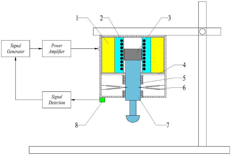
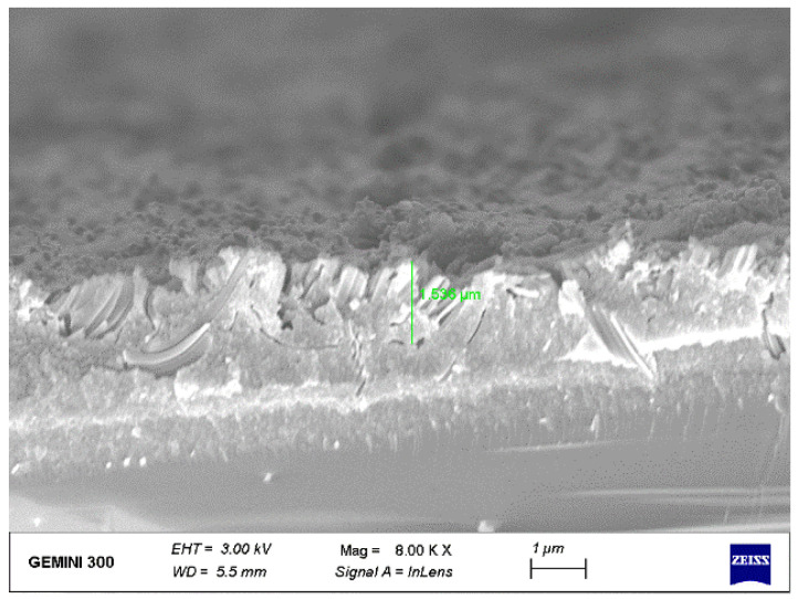
In this work, we design a micro-vibration platform, which combined with the traditional metal-assisted chemical etching (MaCE) to etch silicon nanowires (SiNWs). The etching mechanism of SiNWs, including in the mass-transport (MT) and charge-transport (CT) processes, was explored through the characterization of SiNW's length as a function of MaCE combined with micro-vibration conditions, such as vibration amplitude and frequency. The scanning electron microscope (SEM) experimental results indicated that the etching rate would be continuously improved with an increase in amplitude and reached its maximum at 4 μm. Further increasing amplitude reduced the etching rate and affected the morphology of the SiNWs. Adjusting the vibration frequency would result in a maximum etching rate at a frequency of 20 Hz, and increasing the frequency will not help to improve the etching effects.
Keywords: MaCE; amplitude; etching rate; frequency; micro-vibration platform.
Conflict of interest statement
The authors declare no conflict of interest.
Figures


Similar articles
-
Unraveling the Morphological Evolution and Etching Kinetics of Porous Silicon Nanowires During Metal-Assisted Chemical Etching.Nanoscale Res Lett. 2017 Dec;12(1):385. doi: 10.1186/s11671-017-2156-z. Epub 2017 Jun 2. Nanoscale Res Lett. 2017. PMID: 28582967 Free PMC article.
-
Enhanced photocatalytic activities of silicon nanowires/graphene oxide nanocomposite: Effect of etching parameters.J Environ Sci (China). 2021 Mar;101:123-134. doi: 10.1016/j.jes.2020.08.010. Epub 2020 Aug 25. J Environ Sci (China). 2021. PMID: 33334508
-
Facile and clean release of vertical Si nanowires by wet chemical etching based on alkali hydroxides.Small. 2013 Mar 25;9(6):905-12. doi: 10.1002/smll.201201804. Epub 2012 Nov 23. Small. 2013. PMID: 23180651
-
Silicon Nanowires via Metal-Assisted Chemical Etching for Energy Storage Applications.ChemSusChem. 2025 Jan 14;18(2):e202400777. doi: 10.1002/cssc.202400777. Epub 2024 Sep 18. ChemSusChem. 2025. PMID: 39292438 Review.
-
Voltage- and Metal-assisted Chemical Etching of Micro and Nano Structures in Silicon: A Comprehensive Review.Small. 2024 Aug;20(35):e2400499. doi: 10.1002/smll.202400499. Epub 2024 Apr 21. Small. 2024. PMID: 38644330 Review.
References
-
- Giubertoni D., Paternoster G., Acerbi F., Borrise X., Cian A., Filippi A., Gola A., Guerrero A., Murano F.P., Romanato F., et al. Plasmonic Enhanced Photodetectors for Near Infra-Red Light Detection; Proceedings of the International Convention on Information, Communication and Electronic Technology (MIPRO); Opatija, Croatia. 28 September–2 October 2020; - DOI
-
- Sreejith K., Sharma A.K., Basu P.K., Kottantharayil A. A comprehensive investigation of the potential of metal assisted chemical etched (MACE) nano-textures over conventional micron-sized iso-textures for industrial silicon solar cell applications. Sol. Energy. 2021;230:874–882. doi: 10.1016/j.solener.2021.10.035. - DOI
LinkOut - more resources
Full Text Sources
