. 2023 Sep;621(7977):60-65.
doi: 10.1038/s41586-023-06312-0. Epub 2023 Aug 16.

Proximity superconductivity in atom-by-atom crafted quantum dots

Affiliations

Proximity superconductivity in atom-by-atom crafted quantum dots

Lucas Schneider et al. Nature. 2023 Sep.

Abstract

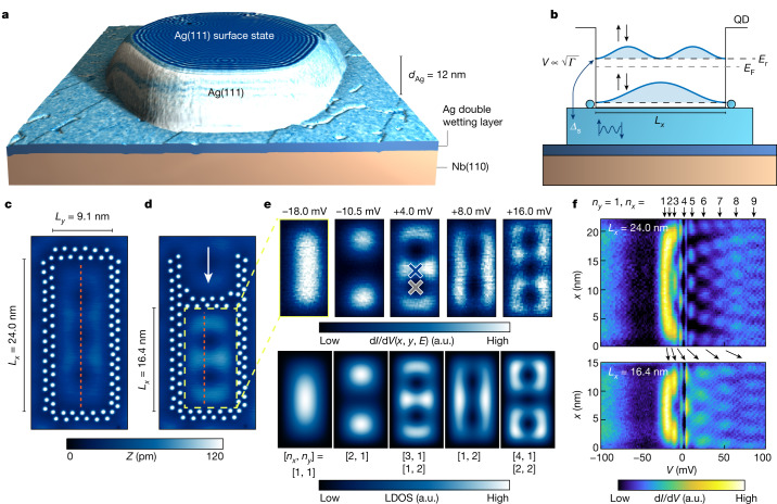
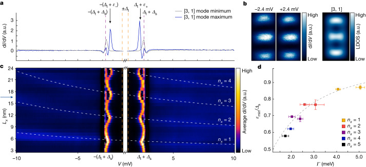
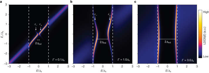
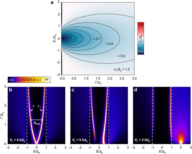
Gapless materials in electronic contact with superconductors acquire proximity-induced superconductivity in a region near the interface1,2. Numerous proposals build on this addition of electron pairing to originally non-superconducting systems and predict intriguing phases of matter, including topological3-7, odd-frequency8, nodal-point9 or Fulde-Ferrell-Larkin-Ovchinnikov10 superconductivity. Here we investigate the most miniature example of the proximity effect on only a single spin-degenerate quantum level of a surface state confined in a quantum corral11 on a superconducting substrate, built atom by atom by a scanning tunnelling microscope. Whenever an eigenmode of the corral is pitched close to the Fermi energy by adjusting the size of the corral, a pair of particle-hole symmetric states enters the gap of the superconductor. We identify these as spin-degenerate Andreev bound states theoretically predicted 50 years ago by Machida and Shibata12, which had-so far-eluded detection by tunnel spectroscopy but were recently shown to be relevant for transmon qubit devices13,14. We further find that the observed anticrossings of the in-gap states are a measure of proximity-induced pairing in the eigenmodes of the quantum corral. Our results have direct consequences on the interpretation of impurity-induced in-gap states in superconductors, corroborate concepts to induce superconductivity into surface states and further pave the way towards superconducting artificial lattices.


Conflict of interest statement

The authors declare no competing interests.

Figures

Fig. 1
Fig. 1. Atom-by-atom built QDs coupled to a superconducting substrate.
a, Three-dimensional rendering of the constant-current STM topography of a Ag island with a thickness of 12 nm. The simultaneously measured dI/dV signal is used as the texture of the model. The island grows on top of a pseudomorphic Ag double layer on Nb(110) (sketched profile; see Methods). b, Sketch of the experimental setup with the QD walls laterally confining the surface-state electrons into spin-degenerate QD eigenmodes of energies Er. The eigenmodes couple to the superconducting substrate (Δs) with a strength VΓ. Er can be pitched by adjusting the width Lx of the QD. c, Constant-current STM image of a rectangular QD with side lengths Lx and Ly consisting of 44 Ag atoms. Lx and Ly are defined as the distance between the Ag atoms in the inner ring. Z, apparent height. d, Constant-current STM image of the same structure with one of the QD walls moved as indicated by the arrow. e, Upper panels, constant-height dI/dV maps at bias voltages indicated in the respective panels measured in the interior of the QD in panel d (area marked by the dashed yellow lines). All panels are 15 × 7.5 nm2 in size. Lower panels, simulation of a hard-wall rectangular box with dimensions Lx = 16.4 nm, Ly = 9.1 nm assuming a parabolic dispersion of the quasiparticles with meff = 0.58me and E0 = −26.4 meV (see Methods). The quantum numbers [nx, ny] of the dominant eigenmodes at the energies of the experimental maps (corrected by an offset of Δtip) are given below each map. f, dI/dV line profiles along the dashed orange vertical lines marked in panels c and d. QD eigenmodes with ny = 1 and nx as indicated by the arrows at the top are observed. Their respective energy is shifted when the length Lx is altered as illustrated by the black arrows. a.u., arbitrary units.
Fig. 2
Fig. 2. In-gap states of near-zero-energy pitched QD eigenmodes.
a, dI/dV spectra measured at two different positions (grey and blue crosses in Fig. 1e) in the QD shown in Fig. 1d–f. The values of the tip’s superconducting gap eV = ±Δt and the sum eV = ±(Δt + Δs) with the proximity-induced Ag bulk gap Δs are marked by dashed orange and purple lines, respectively. In-gap states appear at energies ±(Δt + ε±), marked by black arrows. b, Left, constant-height dI/dV maps measured at the energies of the in-gap state peaks in the same area as in Fig. 1e. Right, particle-in-a-box simulation evaluated at zero energy with dominant contribution of the eigenmode with [nx, ny] = [3, 1]. c, Evolution of averaged dI/dV spectra from dI/dV line profiles measured along the central vertical axis of different QDs (see dashed orange lines in Fig. 1c,d) as a function of Lx. The dashed white lines mark the evolution of the eigenmodes with ny = 1 and nx = {1, 2, 3, 4} obtained from fitting the dI/dV spectra at energies outside the gap (see Supplementary Note 2). The length of the QD presented in panels a and b is marked by the blue arrow on the left side. d, Linewidths Γ of different QD eigenmodes extracted from fitting data from different QDs to Lorentzian peaks at energies outside the gap (see Supplementary Note 2). These are compared with the minimal energies of the in-gap states found when Er ≈ 0 (error bars are standard deviations extracted from fitting the data; see Supplementary Note 2 for details). The dashed grey line is the expected theoretical relation for a spin-degenerate level coupled to a superconducting bath (based on equation (13) in Methods). Data on further QDs constructed and analysed as described in Supplementary Note 3 are included in panel d. a.u., arbitrary units.
Fig. 3
Fig. 3. MSSs from resonance scattering at a spin-degenerate localized level.
a, Energy-dependent local electron density of states LDOS(E) of a single localized level at energy Er coupled to a superconducting bath with the parameter Δs. The coupling strength Γ ∝ V2 (see Methods) equals 0.1Δs. The induced gap Δind and the energies of the in-gap states ε± are marked. b, Same as panel a but for Γ = 1.0Δs. c, Same as panel a but for Γ = 3.0Δs. An energetic broadening of δE = 0.03Δs has been added in all panels (see Methods). a.u., arbitrary units.
Fig. 4
Fig. 4. Particle–hole mixture of the in-gap states.
Bogoliubov angle θB of the in-gap states with different mean energies ε¯=(ε+ε)/2 normalized to their minimal energies εmin. All error bars are standard deviations extracted from fitting the data; see Supplementary Note 2 for details. The dashed grey lines represent the expected relationship for Bogoliubov quasiparticles with an induced gap of Δind = εmin as derived from the effective Hamiltonian in equation (2) (see Methods for details). Inset, Bogoliubov quasiparticles are coherent combinations of electrons (filled circle) and holes (empty circle). The Bogoliubov angle θB of a quasiparticle quantifies the amount of particle–hole mixing.
Extended Data Fig. 1
Extended Data Fig. 1. Complete set of dI/dV line profiles measured on 34 different QDs.
dI/dV line profiles measured along the central vertical axis of 34 different QDs with lengths Lx ranging from 3.0 nm up to 24.0 nm. All line profiles have been measured at constant tip height. Parameters: Vstab = −15 mV, Istab = 4 nA, Vmod = 50 µV.
Extended Data Fig. 2
Extended Data Fig. 2. MSS energy versus localized level energy Er and coupling strength Γ to the superconducting host.
a, Energy of the lowest-energy excitation of the Hamiltonian in equation (1). For all Γ ≠ 0, an in-gap solution with ε+/Δs < 1 is found. bd, Energy-dependent local electron density of states LDOS(E) of a spin-degenerate localized level at energy Er/Δs = 0.0 (panel b), Er/Δs = 0.5 (panel c) and Er/Δs = 2.0 (panel d) coupled to a superconducting bath with the order parameter Δs by a coupling strength Γ ∝ V2 (see Methods). An energetic broadening of δE = 0.03Δs has been added in all panels (see Methods).
Extended Data Fig. 3
Extended Data Fig. 3. Dependence of MSS energy on the localized level energy Er for individual QD eigenmodes.
a, Evolution of averaged dI/dV spectra from dI/dV line profiles measured along the central vertical axis of different QDs (same data as Fig. 2c) as a function of the localized level energy Er of the nx = 1 resonance. The value of Er has been extrapolated from inserting the known QD length into the fit function for Er(Lx) obtained in Supplementary Note 2. b, Energy-dependent local electron density of states LDOS(E) of a single localized level at energy Er coupled to a superconducting bath with the parameter Δs = 1.35 meV. The coupling strength Γ is set to 4.06 meV, motivated by the average experimental width of the nx = 1 resonances taken from Fig. 2d. c,d, Same as panels a and b but for the nx = 2 resonances and Γ = 2.58 meV. e,f, Same as panels a and b but for the nx = 3 resonances and Γ = 2.02 meV. An energetic broadening of δE = 0.08 meV corresponding to the experimental energy resolution has been added in all theoretical panels (see Methods).
Extended Data Fig. 4
Extended Data Fig. 4. Bogoliubov angle of individual eigenmodes compared with the MSS model.
a, Bogoliubov angle θB of the in-gap states of the nx = 1 eigenmode with different mean energies ε¯=(ε+ε)/2. All error bars are standard deviations extracted from fitting the data; see Supplementary Note 2 for details. The coloured lines represent the energy-dependent Bogoliubov angles of MSSs computed numerically from the LDOS in equation (13) in Methods. Here we use Γ = 4.55 meV as extracted on average for all nx = 1 eigenmodes (see Supplementary Note 2) and the experimental value Δs = 1.35 meV. The dashed grey lines represent the expected relationship for Bogoliubov quasiparticles (equation (27)) with an induced gap of Δind = εmin set to the value given by the induced gap of the MSS model using the values for Γ and Δs above. b, The same for the nx = 2 eigenmodes and Γ = 2.82 meV. c, nx = 3 eigenmodes, Γ = 2.20 meV. d, nx = 4 eigenmodes, Γ = 1.96 meV. e, nx = 5 eigenmodes, Γ = 1.73 meV. The sample gap Δs is marked by the light blue dashed lines in all panels.
Extended Data Fig. 5
Extended Data Fig. 5. Growth of Ag on Nb(110).
a, Constant-current STM image of a thin Ag island grown on oxygen-reconstructed Nb(110). The apparent height of the island equals 540 pm, indicating that Ag grows in double layers (DL). The white bar corresponds to 2 nm. b, dI/dV spectra measured on the Ag DL and on the oxidized Nb(110) substrate. The sharp peaks at bias voltages corresponding to ±(Δt + Δs) and ±(Δt − Δs) are marked by purple arrows. c, Large-scale constant-current image of a sample with nominal Ag coverage of 8ML. The DL is found to cover the entire Nb surface and further thicker Ag(111) islands are formed. The white bar corresponds to 500 nm. d, Zoom-in on the DL surface quality, exhibiting atomically flat areas of Ag and several twofold symmetric defects of unknown origin. The white bar corresponds to 2 nm. e, Atomically resolved constant-current image of the same area shown in panel d. Inset, Fourier transform of the atomic-resolution image, showing Bragg spots incompatible with a hexagonal lattice (a perfect hexagon is overlaid as a yellow dashed line) but with a pseudomorphic growth on the bcc(110) surface of clean Nb. The white bar corresponds to 2 nm. f, Atomically resolved constant-current image of a thick Ag island. The white bar corresponds to 2 nm. Inset, Fourier transform of the image, showing Bragg spots in good agreement with a hexagonal fcc(111) growth. Parameters: V = 5 mV, I = 1 nA for panel a; Vstab = 5 mV, Istab = 1 nA, Vmod = 50 µV for panel b; V = 1,000 mV, I = 0.1 nA for panel c; V = 2.5 mV, I = 10 nA for panel d; V = 2.5 mV, I = 80 nA for panel b; V = 100 mV, I = 1 nA for panel f.
Extended Data Fig. 6
Extended Data Fig. 6. Low-energy electronic structure of Ag(111)/Nb(110).
a, Large-scale constant-current STM image of a 12 nm thin Ag island. The black bar corresponds to 20 nm. b, dI/dV map at above-gap energy acquired with constant tip height and on the same region shown in panel a. The insets show the Fourier transform (FFT) of the dI/dV map. Parameters: V = −100 mV, I = 1 nA for panel a; Vstab = 10 mV, Istab = 2 nA, Vmod = 100 µV for panel b.
Extended Data Fig. 7
Extended Data Fig. 7. Single Ag atoms on Ag(111)/Nb(110).
a, Constant-current STM image of a clean Ag area. The white bar corresponds to 10 nm. be, The same area after approaching the tip by 600 pm towards the surface at different positions. A single adsorbate of similar apparent height is found after each approach with the tip, consistent with the finding of ref. . Therefore, we identify these adsorbates as single Ag atoms. f, Constant-current STM image of a QD’s wall consisting of Ag atoms manipulated to form a suitable shape of the wall. The white bar corresponds to 2 nm. g, dI/dV spectra measured on three of the Ag atoms marked in panel f (yellow, purple and red) as well as on the surface between the atoms (grey). Parameters: V = 15 mV, I = 1 nA for panels ae; V = 5 mV, I = 1 nA for panel f; Vstab = −5 mV, Istab = 1 nA, Vmod = 50 µV for panel g.

References

    1. de Gennes PG. Boundary effects in superconductors. Rev. Mod. Phys. 1964;36:225–237. doi: 10.1103/RevModPhys.36.225. - DOI
    1. Buzdin AI. Proximity effects in a superconductor/ferromagnet junction. J. Phys. Chem. Solids. 2008;69:3257–3260. doi: 10.1016/j.jpcs.2008.06.063. - DOI
    1. Schneider L, et al. Topological Shiba bands in artificial spin chains on superconductors. Nat. Phys. 2021;17:943–948. doi: 10.1038/s41567-021-01234-y. - DOI
    1. Kezilebieke S, et al. Topological superconductivity in a van der Waals heterostructure. Nature. 2020;588:424–428. doi: 10.1038/s41586-020-2989-y. - DOI - PubMed
    1. Jäck B, et al. Observation of a Majorana zero mode in a topologically protected edge channel. Science. 2019;364:1255–1259. doi: 10.1126/science.aax1444. - DOI - PubMed