. 2023 Aug 30;15(34):40709-40718.
doi: 10.1021/acsami.3c04808. Epub 2023 Aug 22.

Novel Mixed-Dimensional hBN-Passivated Silicon Nanowire Reconfigurable Field Effect Transistors: Fabrication and Characterization

Affiliations

Novel Mixed-Dimensional hBN-Passivated Silicon Nanowire Reconfigurable Field Effect Transistors: Fabrication and Characterization

Sayantan Ghosh et al. ACS Appl Mater Interfaces. .

Abstract

This work demonstrates the novel concept of a mixed-dimensional reconfigurable field effect transistor (RFET) by combining a one-dimensional (1D) channel material such as a silicon (Si) nanowire with a two-dimensional (2D) material as a gate dielectric. An RFET is an innovative device that can be dynamically programmed to perform as either an n- or p-FET by applying appropriate gate potentials. In this work, an insulating 2D material, hexagonal boron nitride (hBN), is introduced as a gate dielectric and encapsulation layer around the nanowire in place of a thermally grown or atomic-layer-deposited oxide. hBN flake was mechanically exfoliated and transferred onto a silicon nanowire-based RFET device using the dry viscoelastic stamping transfer technique. The thickness of the hBN flakes was investigated by atomic force microscopy and transmission electron microscopy. The ambipolar transfer characteristics of the Si-hBN RFETs with different gating architectures showed a significant improvement in the device's electrical parameters due to the encapsulation and passivation of the nanowire with the hBN flake. Both n- and p-type characteristics measured through the top gate exhibited a reduction of hysteresis by 10-20 V and an increase in the on-off ratio (ION/IOFF) by 1 order of magnitude (up to 108) compared to the values measured for unpassivated nanowire. Specifically, the hBN encapsulation provided improved electrostatic top gate coupling, which is reflected in the enhanced subthreshold swing values of the devices. For a single nanowire, an improvement up to 0.97 and 0.5 V/dec in the n- and p-conduction, respectively, is observed. Due to their dynamic switching and polarity control, RFETs boast great potential in reducing the device count, lowering power consumption, and playing a crucial role in advanced electronic circuitry. The concept of mixed-dimensional RFET could further strengthen its functionality, opening up new pathways for future electronics.

Keywords: ambipolar; flash lamp annealing; hBN encapsulation; mixed-dimensional reconfigurable FET; nickel silicide; subthreshold swing.


Conflict of interest statement

The authors declare no competing financial interest.

Figures

Figure 1
Figure 1
Ambipolar RFET characteristics (a) typical IV characteristics of a silicon nanowire RFET (b) energy band diagram of an ambipolar RFET under biased condition showing (1) hole conduction by tunneling with upward band bending, (2) off-state region dominated by high energy charge carrier conduction, and (3) electron conduction by tunneling with downward band bending.
Figure 2
Figure 2
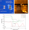
AFM characterization of the fabricated devices. (a) Visible light micrograph of two different single silicon nanowire devices with and without hBN dielectric layer. (b) AFM scan of the fabricated devices is shown in image (a). Lines 1, 2, and 3 are three different line profiles for determining the thickness of the hBN flake. (c) Thickness of hBN is based on the height profile lines 1, 2, and 3 in the image (b). Thickness of the hBN flake shown here is approximately 10 nm.
Figure 3
Figure 3
(a) Bright-field TEM micrograph of a sectioned nanowire device. The device structure consists of a buried SiO2 layer underneath the silicon nanowire. On top of the nanowire channel is the hBN dielectric, which is shown to cover the nanowire. A stack of Ti and Al serves as the gate electrodes above the hBN. (b) Corresponding superimposed EDXS-based element distribution maps of the hBN-silicon-nanowire-based device.
Figure 4
Figure 4
(a) Cross-sectional view of the device, including the voltage naming conventions used in this work. The device structure consists of a bottom Si layer on top of which is a 100 nm buried SiO2 layer. The single nanowire is fabricated on top of the buried oxide layer. Ni contact pads are placed on both sides of the Si nanowire. Annealing creates NixSiy Schottky junctions in the nanowire. hBN is transferred on top of the device as the gate dielectric. A bilayer of Ti and Al serves as the top gate for the device. (b) Transfer characteristics of a single silicon nanowire-based device comprising an hBN flake as the dielectric layer. Different gating schemes are incorporated to deduce the IV characteristics. The length and width of the nanowire are 3 μm and 25 nm, respectively. The arrows in the transfer characteristics denote the direction of the curve based on the gate voltage sweep.
Figure 5
Figure 5
Transfer characteristics of a device consisting of a nanowire array. hBN is used as a dielectric layer. The lengths and widths of the nanowires are 3 μm and 25 nm, respectively. The pitch between the nanowires is 200 nm. The black curve shows a straight line below −20 V due to the compliance set in the measurement tool. For the rest of the transfer characteristics, the compliance was set at a higher drain current value. Similar to Figure 4b, the arrows in the transfer characteristics denote the direction of the curve based on the gate voltage sweep.
Figure 6
Figure 6
A schematic representation of the top-down fabrication process flow of the novel mixed-dimensional RFET device. (i) Starting with SOI substrate, a negative resist HSQ is spin-coated for patterning with EBL, (ii) development of HSQ resist creates the HSQ patterns in the shape of the nanowire, (iii) HSQ patterns are then transferred to the top 20 nm device layer using anisotropic reactive ion etching, (iv) HF dip is carried out to remove the top HSQ later, (v) source and drain Ni contact pads are fabricated by EBL, metal deposition, and lift-off technique, (vi) FLA creates the NiSi2 Schottky junction inside the nanowire, (vii) exfoliated hBN is transferred onto the device by dry-stamping technique, and (viii) top gates are fabricated on top of the hBN layer by EBL, metal deposition, and lift-off.
Figure 7
Figure 7
(a) Transfer of hBN flake indicating the steps of drop-down and peel-off process onto the silicon nanowire-based devices using the dry viscoelastic stamping transfer technique. (b) Visible-light micrograph image of a transferred hBN flake on a single silicon nanowire-based device showing the architecture of contact pads and connection lines. (c) Visible-light micrograph image of a mixed-dimensional RFET device with a top-gate present on the hBN layer.

References

    1. Simon M.; Heinzig A.; Trommer J.; Baldauf T.; Mikolajick T.; Weber W. M. Top-down Technology for Reconfigurable Nanowire FETs with Symmetric On-Currents. IEEE Trans. Nanotechnol. 2017, 16, 812–819. 10.1109/TNANO.2017.2694969. - DOI
    1. Heinzig A.; Slesazeck S.; Kreupl F.; Mikolajick T.; Weber W. M. Reconfigurable Silicon Nanowire Transistors. Nano Lett. 2012, 12, 119–124. 10.1021/nl203094h. - DOI - PubMed
    1. Mikolajick T.; Galderisi G.; Rai S.; Simon M.; Böckle R.; Sistani M.; Cakirlar C.; Bhattacharjee N.; Mauersberger T.; Heinzig A.; et al. Reconfigurable Field Effect Transistors: A technology Enablers Perspective. Solid-State Electron. 2022, 194, 108381.10.1016/j.sse.2022.108381. - DOI
    1. Lin Y.-M.; Appenzeller J.; Knoch J.; Avouris P. High-Performance Carbon Nanotube Field-Effect Transistor with Tunable Polarities. IEEE Trans. Nanotechnol. 2005, 4, 481–489. 10.1109/TNANO.2005.851427. - DOI
    1. Lin Y.-M.; Chiu H.-Y.; Jenkins K. A.; Farmer D. B.; Avouris P.; Valdes-Garcia A. Dual-Gate Graphene FETs with f_{T} of 50 GHz. IEEE Electron Device Lett. 2010, 31, 68–70. 10.1109/led.2009.2034876. - DOI