. 2023 Aug 9;8(33):30621-30629.
doi: 10.1021/acsomega.3c04256. eCollection 2023 Aug 22.

Structural, Optical, and Electrical Properties of Hafnium-Aluminum-Zinc-Oxide Films Grown by Atomic Layer Deposition for TCO Applications

Affiliations

Structural, Optical, and Electrical Properties of Hafnium-Aluminum-Zinc-Oxide Films Grown by Atomic Layer Deposition for TCO Applications

Maciej Krajewski et al. ACS Omega. .

Abstract

ZnO is a widely studied material that exhibits versatile doping possibilities. Most research presents singly doped ZnO, leaving the potential of codoping unexplored. Within this study, hafnium-aluminum codoped zinc oxide (HAZO) thin films were grown on a glass substrate using the atomic layer deposition technique at 200 °C. A comprehensive analysis of the surface morphology and electrical and optical properties of the samples was conducted for varying the Al/Hf doping ratio. X-ray diffraction studies showed that the obtained films are polycrystalline, exhibiting a preferential growth direction along the (1 0 0) plane without any detectable precipitates. Moreover, the electrical measurements of HAZO films revealed that they exhibit lower resistivity (∼9.5 × 10⁻⁴ Ωcm) than the commonly used aluminum zinc oxide films (AZO). This improvement can be primarily attributed to the promotion of the n-type carrier concentration to 4.45 × 1020 cm-3 while maintaining a mobility value equal to 14.7 cm2/Vs. The doping also influences the optical properties of the material by widening the band gap and changing the refractive index, as observed by spectroscopy and ellipsometry studies. These findings highlight the potential of proposed HAZO thin films for future applications in electronic devices utilizing transparent conducting oxides.


Conflict of interest statement

The authors declare no competing financial interest.

Figures
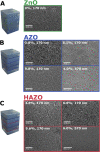
Figure 1
Figure 1
SEM images of (A–C) ZnO, AZO, and HAZO samples (170 and 570 nm thickness) with different dopant contents. On the left, the schematic drawings of the sample structure are shown, depicting the dopant relative positions during growth (aluminum as blue and hafnium as red stripes).
Figure 2
Figure 2
Granulometry results obtained from SEM images for both types of dopant samples with varying concentrations. On the right of each histogram, the average value of the grain length along with the standard deviation is presented.
Figure 3
Figure 3
AFM 3D images showing the surface morphology of each sample with different dopant concentrations.
Figure 4
Figure 4
X-ray diffractograms of as deposited AZO (left) and HAZO (right) selected thin films on the glass substrates with a different dopant content. ZnO results are shown as the reference.
Figure 5
Figure 5
Intensity relationship between (002) and (100) peaks in AZO and HAZO samples showing the preferred orientation of the crystallites in the thin film. The dotted line represents the theoretical threshold for either a- or c-axis oriented sample. Pure ZnO is marked as a green square.
Figure 6
Figure 6
Electrical parameters of the studied materials for varying cation metal contents. Pure ZnO sample (i.e., with 0% doping) is indicated with a green square. The stars indicate the 570 nm AZO (blue) and HAZO (red) samples.
Figure 7
Figure 7
Optical transmittance spectra of (A) AZO and (B) HAZO thin films with different dopant concentrations deposited on a glass substrate (included in the graph).
Figure 8
Figure 8
Tauc plots of (A) AZO and (B) HAZO thin films with varying dopant concentrations obtained from transmittance spectra together with linear fits pointing toward optical band gap value (dashed lines). (C) Optical band gap values determined from the Tauc plot for corresponding samples. Dashed lines are a guide to the eye. (D) Calculated band gap widening and narrowing effects. Dashed lines are calculated according to eq 2. Carrier concentrations are obtained from Hall measurements.
Figure 9
Figure 9
Complex dielectric functions of (A, B) AZO and (C, D) HAZO for various dopant concentrations extracted from the ellipsometric measurements. The red line refers to the optical constants of ZnO.

References

    1. Zhao B.; Bai S.; Kim V.; Lamboll R.; Shivanna R.; Auras F.; Richter J. M.; Yang L.; Dai L.; Alsari M.; She X. J.; Liang L.; Zhang J.; Lilliu S.; Gao P.; Snaith H. J.; Wang J.; Greenham N. C.; Friend R. H.; Di D. High-Efficiency Perovskite–Polymer Bulk Heterostructure Light-Emitting Diodes. Nat. Photonics 2018, 12, 783–789. 10.1038/s41566-018-0283-4. - DOI
    1. Li Y.; Meng L.; Yang Y.; Xu G.; Hong Z.; Chen Q.; You J.; Li G.; Yang Y.; Li Y. High-Efficiency Robust Perovskite Solar Cells on Ultrathin Flexible Substrates. Nat. Commun. 2016, 7, 10214.10.1038/ncomms10214. - DOI - PMC - PubMed
    1. De Wolf S.; Holovsky J.; Moon S. J.; Löper P.; Niesen B.; Ledinsky M.; Haug F. J.; Yum J. H.; Ballif C. Organometallic Halide Perovskites: Sharp Optical Absorption Edge and Its Relation to Photovoltaic Performance. J. Phys. Chem. Lett. 2014, 5, 1035–1039. 10.1021/jz500279b. - DOI - PubMed
    1. Cho M.; Eom T.; Nundy S.; Park J. S.; Lee H. J. Conductometric Nitrogen Dioxide Gas Sensors Based on Sol-Gel-Prepared Hafnium-Added Indium Zinc Oxide (Hf-IZO). Sens. Actuators B Chem. 2021, 344, 13019810.1016/j.snb.2021.130198. - DOI
    1. Kim W.; Choi M.; Yong K. Generation of Oxygen Vacancies in ZnO Nanorods/Films and Their Effects on Gas Sensing Properties. Sens. Actuators B Chem. 2015, 209, 989–996. 10.1016/j.snb.2014.12.072. - DOI