. 2023 Dec;18(12):1430-1438.
doi: 10.1038/s41565-023-01484-2. Epub 2023 Sep 4.

Microwave synthesis of molybdenene from MoS2

Affiliations

Microwave synthesis of molybdenene from MoS2

Tumesh Kumar Sahu et al. Nat Nanotechnol. 2023 Dec.

Abstract

Dirac materials are characterized by the emergence of massless quasiparticles in their low-energy excitation spectrum that obey the Dirac Hamiltonian. Known examples of Dirac materials are topological insulators, d-wave superconductors, graphene, and Weyl and Dirac semimetals, representing a striking range of fundamental properties with potential disruptive applications. However, none of the Dirac materials identified so far shows metallic character. Here, we present evidence for the formation of free-standing molybdenene, a two-dimensional material composed of only Mo atoms. Using MoS2 as a precursor, we induced electric-field-assisted molybdenene growth under microwave irradiation. We observe the formation of millimetre-long whiskers following screw-dislocation growth, consisting of weakly bonded molybdenene sheets, which, upon exfoliation, show metallic character, with an electrical conductivity of ~940 S m-1. Molybdenene when hybridized with two-dimensional h-BN or MoS2, fetch tunable optical and electronic properties. As a proof of principle, we also demonstrate applications of molybdenene as a surface-enhanced Raman spectroscopy platform for molecular sensing, as a substrate for electron imaging and as a scanning probe microscope cantilever.


Conflict of interest statement

The authors declare no competing interests.

Figures

Fig. 1
Fig. 1. Experimental realization of molybdenene.
a, Schematic diagram depicting graphene-catalysed microwave synthesis of molybdenene sheet (intense electric field breaks Mo–S bonds and Mo atoms move out through the expanded graphene network), Mo, S and C atoms are represented in pink, yellow and grey respectively, b,c, FESEM images of flat atomic sheets obtained by sonication followed by centrifugation of Mo whiskers. d,e, AFM images showcasing staircase-like features (each step being 0.4 nm) indicative of screw-dislocation-mediated growth of Mo whiskers (d,e) and showing monolayer Mo sheet, that is, molybdenene, transferred onto SiO2 substrate (f). g, Large-area HAADF image, which is taken to acquire EELS in the marked green region. h, EELS spectrum of synthesized Mo sheets in the high-loss region ranging from 2,400 to 3,300 eV. Int. intensity; a.u., arbitrary units. i, EELS spectrum ranging from 0 to 400 eV showing a zero-loss peak and low-loss plasmon oscillation peaks. j, EELS spectrum acquired in the high-loss region (200–450 eV) depicting a highly intense M4 peak.
Fig. 2
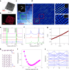
Fig. 2. Structural details and electronic character.
a,b, TEM imaging of formed molybdenene sheet and elemental mapping. c, HRTEM image of top surface of molybdenene. d, Zoomed-in image of marked region in c. Criss-cross patterns of atoms are observed with four-fold symmetry (region 1 in d) and hexagonal arrangements of atoms with sixfold symmetry (region 2 in d). e, Raman spectra of as-synthesized Mo whiskers and surface attained after subsequent peeling of top layer. The bottom spectrum for the final peeling step clearly shows distinct Raman peaks at ~405 cm−1, which is characteristic of metallic phase, and its second overtone at ~810 cm−1. For visual clarity oxide Raman peaks are red shaded and metallic Raman peaks are green shaded. Distinct metallic Raman signatures and flat sheets observed in FESEM, TEM and AFM establish synthesis of free-standing molybdenene. f, Layer dependence of molybdenene Raman spectra. g, IV characteristics of Mo sheet placed on SiO2 substrate. h, Molybdenene structure with fourfold symmetry obtained using DFT calculations. i, The minimum-energy curve to determine equilibrium interlayer separation for molybdenene surface with fourfold symmetry. j, DFT band structure calculations of fourfold structure of molybdenene.
Fig. 3
Fig. 3. Atomic-resolution HAADF STEM imaging.
a,b, Low-magnification HAADF STEM images of molybdenene highlighting the electron-transparent nature of the sheets. Stacked atomic layers are visible. c,d,g,h, High-resolution HAADF STEM images of different areas along with atomistic line profiles. Dist., distance. e,f, High-resolution cross-sectional images of molybdenene atomic sheets. Fourfold atomic arrangements are observed. i,j, Layer-dependent resolved images along with zoomed-in images in selected locations 1–3.
Fig. 4
Fig. 4. Applications of molybdenene.
a, Optical images of fabricated and commercially available cantilevers. Top left inset: FESEM image of a typical molybdenene sheet used for cantilever fabrication. Top right inset: schematic depiction of parallel and perpendicular orientations of molybdenene sheets. b, Amplitude and phase versus frequency plots of a fabricated cantilever. ch, Comparison of topography images of standard calibration grid (c,d), 2D structure of molybdenene sheets (e,f) and DNA on graphene oxide sheets (g,h) obtained with fabricated and commercial cantilevers, respectively. i,j, SEM images of Mo cantilevers (inset: amplitude (V) versus frequency (Hz) sweep before (green curve) and after (red curve) DNA attachment) for molybdenene-fabricated tips of two different dimensions (length and breadth). k,l, SEM images of multiwalled carbon nanotubes over glass and molybdenene as an anchoring substrate respectively.
Fig. 5
Fig. 5. Molybdenene-based 2D–2D hybrids.
a, Raman spectrum of synthesized M–BN hybrid and a digital image with UV light exposure (inset). b, TEM image of M–BN. ce, Elemental mapping showing M–BN, boron, nitrogen and Mo. f, HRTEM image showing intertwined atomic arrangements. g, The atomic line profile of f as marked by the white and red lines has average interatomic distances of 0.35 nm and 0.35 nm. h, Tauc plot for optical band gap of M–BN hybrid. i, IV/PC behaviour of M–BN hybrid. Red and green lines corresond to current signal under red or green laser illumination, respectively. j, Raman spectrum of synthesized M–MoS2 hybrid and a digital image with UV light exposure (inset). k,l, Elemental mapping of M–MoS2 hybrid, showing the presence of Mo and S. m, TEM image of M–MoS2. n, HRTEM image taken at the intersection of two layers. o, Zoomed-in HRTEM image of region 1 marked in n (inset: FFT pattern). p, The atomic line profile of o has average interatomic distances 0.31 (green plot) and 0.30 nm (red plot). q, Optical band gap plot of Mo–MoS2 hybrid. r, IV/PC measurements of M–MoS2 hybrid. Blue and red lines corresond to current signal under blue or red laser illumination, respectively.

References

    1. Novoselov, K. S. et al. Electric field in atomically thin carbon films. Science306, 666–669 (2004). - PubMed
    1. Mannix, A. J. et al. Synthesis of borophenes: anisotropic, two-dimensional boron polymorphs. Science350, 1513–1516 (2015). - PMC - PubMed
    1. Feng, B. et al. Experimental realization of two-dimensional boron sheets. Nat. Chem.8, 563–568 (2016). - PubMed
    1. Ranjan, P. et al. Freestanding borophene and its hybrids. Adv. Mater.31, 900353 (2019). - PubMed
    1. Hanlon, D. et al. Liquid exfoliation of solvent-stabilized few-layer black phosphorus for applications beyond electronics. Nat. Commun.6, 8563 (2015). - PMC - PubMed