Review
. 2023 Aug 28;13(17):2443.
doi: 10.3390/nano13172443.

Recent Advances in Cerium Oxide-Based Memristors for Neuromorphic Computing

Affiliations
Review

Recent Advances in Cerium Oxide-Based Memristors for Neuromorphic Computing

Sarfraz Ali et al. Nanomaterials (Basel). .

Abstract

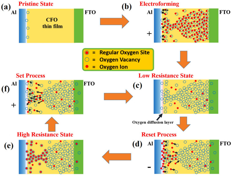
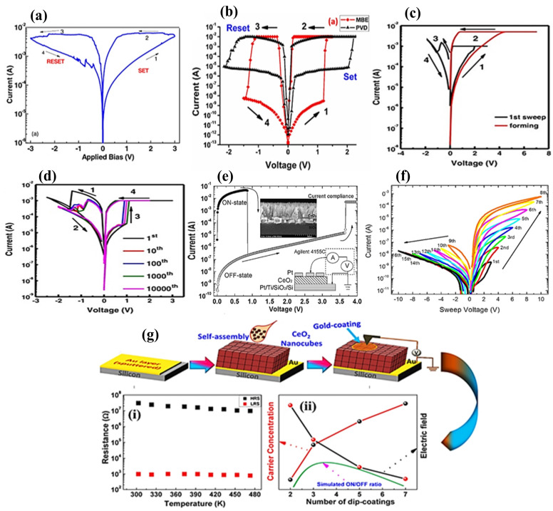
This review article attempts to provide a comprehensive review of the recent progress in cerium oxide (CeO2)-based resistive random-access memories (RRAMs). CeO2 is considered the most promising candidate because of its multiple oxidation states (Ce3+ and Ce4+), remarkable resistive-switching (RS) uniformity in DC mode, gradual resistance transition, cycling endurance, long data-retention period, and utilization of the RS mechanism as a dielectric layer, thereby exhibiting potential for neuromorphic computing. In this context, a detailed study of the filamentary mechanisms and their types is required. Accordingly, extensive studies on unipolar, bipolar, and threshold memristive behaviors are reviewed in this work. Furthermore, electrode-based (both symmetric and asymmetric) engineering is focused for the memristor's structures such as single-layer, bilayer (as an oxygen barrier layer), and doped switching-layer-based memristors have been proved to be unique CeO2-based synaptic devices. Hence, neuromorphic applications comprising spike-based learning processes, potentiation and depression characteristics, potentiation motion and synaptic weight decay process, short-term plasticity, and long-term plasticity are intensively studied. More recently, because learning based on Pavlov's dog experiment has been adopted as an advanced synoptic study, it is one of the primary topics of this review. Finally, CeO2-based memristors are considered promising compared to previously reported memristors for advanced synaptic study in the future, particularly by utilizing high-dielectric-constant oxide memristors.

Keywords: CeO2; RRAM memristive devices; capping layers; filamentary mechanisms; neuromorphic learning systems; switching layers; symmetric and asymmetric electrodes; synaptic devices.


Conflict of interest statement

The authors declare that they have no known competing financial interest or personal relationships that could have appeared to influence the work reported in this paper.

Figures

Figure 1
Figure 1
(a) TEM result for the cell containing a larger electrode showing a space after the forming process (scale bar: 200 nm). The red color square and zoomed-in image of the filament (indicated with the upper arrows) close to the dielectric/inert electrode edge (scale bar: 20 nm) and (b) The red color square and zoomed-in image and TEM image after erasing. Adopted from [52]. Copyright 2012 Nature Publishing Group. Conductance quantization with the synaptic trend of Ta2O5-based atomic switching: (c) observed increment in quantized conductance owing to the cell upon application of positive voltage pulses of width 20 ms during a 2-s interval. The inset shows the controlled-conductance level realized by inserting a series combination with the cell along with a current-controlling resistor with a resistance of 3 kΩ, (d) observed decrement in quantized conductance owing to the cell upon application of negative voltage pulses of width 20 ms during a 2-s interval. The input pulses are directly connected to the device, shown in the inset view, and (e) The quantized conductance histogram demonstration from measured data with zoomed-in image of conductance against time. Adopted from [53]. Copyright 2012 IOP Publishing.
Figure 3
Figure 3
Schematic depiction of thermochemical process showing the RS of (a) pristine state, HRS under (b) Joule heating and (c) pyrolysis, (d) set process associated with conducting channel creation, LRS under (e) Joule heating, (f) reset process associated with CF breakdown, and (g) reversion to the set process. Adopted from [67]. Copyright 2018 John Wiley & Sons, Ltd.
Figure 6
Figure 6
(a) Demonstration of electrochemical process for the creation and rupture of conducting silver filaments corresponding to log (I)–V characterization for the Ag/Ti/CeO2/Pt structure. (b) Schematic depiction of the URS for the Ag/Ti/CeO2/Pt device, with I–V graphs for this memory device indicating unipolar operation trend. Adopted from [32]. Copyright 2020 Elsevier B.V. (c) Schematic illustration of the conducting channels in a TaN/CeO2/TiO2/Pt cell with corresponding graphs showing ideal BRS behavior at annealing temperatures of 350 °C, 450 °C, 500 °C, and 550 °C. Adopted from [76]. Copyright 2017 Elsevier B.V.
Figure 9
Figure 9
(a) Energy band diagram for semiconducting metal interface and surface states at different reverse biases. (b) Ce 3d deconvolution XPS results for 30-s sputtering sample. I–V trends for samples with fitting curves: (c) Schottky emission fitting curves, (d) Schottky emission fitting lines, (e) F–N tunneling fitting lines. Adopted from [81]. Copyright 2022 Elsevier B.V. (f) Schematic display of Schottky barrier-height tunning occurring at the CeO2/Pt junction by OV redistribution when positive voltages are applied to the top Pt- electrode, extracting OVs near the bottom contact. (g) I–V curves of the reference device under annealing of Pt/SiO2/CeO2/SiO2/Pt cell at 500 °C. (h) XPS spectra of the Ce 3d levels for nonannealing and at 400 °C, 500 °C, and 600 °C annealing for Pt/CeO2/Pt memristors. (i) Retention performance of Pt/CeO2/Pt memristors at 500 °C annealing upon repeated application of +3–+7 V pulses with 30 repetitions and measurement of current during 1800 s. Adopted from [26] Copyright 2022. Elsevier B.V. (j) Arrangement schematic of the ITO/CeO2/ITO device with I–V curves showing the starting forming mechanism with prior sweeping of the BRS trend for ITO/CeO2/ITO devices containing CeO2-layers with different thicknesses: (k) 15 and (l) 20 nm. (m) Endurance performance of the ITO/CeO2/ITO device. Adopted from [80] Copyright 2015 Elsevier B.V.
Figure 11
Figure 11
(a) Typical RS performance of the W/CeO2 (20 nm)/TiN and W/CeO2 (20 nm)/Si (1 nm)/TiN devices, (b) comparison of HRS and LRS during 50 cycles for RRAMs with and without 1-nm Si buffer layer. Device stability window without and with Si (distinguishable window greater than 10). Adopted from [87]. Copyright 2012 Elsevier B.V. (c) SEM photographs, (d) schematic view of Ag/CeO2/La0.5Sr0.5CoO3 decorated over sapphire substrate and analyzed by the focused ion beam technique, and (e) typical I–V measurements under electrical forming for various cell sizes. Adopted from [88]. Copyright 2014 Elsevier B.V. (f) Schematic demonstration of oxygen (O2−) ion movement in the metal/CeO2-x/La0.8Sr0.2MnO3 cell. (g) Graphical representation of the probe scanning over Ag electrodes for CeO2/La0.8Sr0.2MnO3, the forming step is needed to induce the BRS, which is maintained at low voltage operation. (h) Endurance cycling measurement of LSMO structures. The resistance ratio covering the range of 102–103 with a −1V read voltage is measured. The supplementary view representing successive memory functioning in 100 cycles is observed. Adopted from [91]. Copyright 2015 Elsevier B.V. Schematic representation of the RS mechanism (i) without annealing and (j) annealing treatment in TiN/ZnO/CeO2-x/Pt structures [92]. Copyright 2018 Elsevier B.V.
Figure 2
Figure 2
Schematic illustration of (a) original state containing electrodes as top Al and bottom FTO, (b) electroforming mechanism, (c) LRS-containing conducting cobalt ferrite film and oxygen diffusion layer toward the Al electrode, (d) reset state showing O−2 ions returning and originating from oxygen spreading layer toward the cobalt ferrite film, (e,f) HRS with the set process. Adopted from [58]. Copyright 2017 Nature Publishing Group.
Figure 4
Figure 4
Schematic of (I–V) switching performance of memristors for (a) unipolar type, (b) bipolar type, and for compliance current (CC). Adopted from [69]. Copyright 2016 Walter de Gruyter GmbH.
Figure 5
Figure 5
(a) Typical semilogarithmic I–V curves of the Au/CeO2/ITO device. Adopted from [70]. Copyright 2012 IOP Publishing. (b) Typical DC sweep I–V characteristics of the Al/CeO2/Au cell. The order of the arrows discloses the sweeping path with numbers. The value of 1 μm indicates the diameter of each device lying between Au (30 nm), CeOx (13 nm), and Au (30 nm). Adopted from [15]. Copyright 2015 American Institute of Physics. Typical bipolar-mode I–V curves indicating the RS trend for the Zr/CeOx/Pt structure containing CeOx layers with different thicknesses: (c) 25 and (d) 14 nm. Adopted from [16], Copyright 2014 Springer Nature. (e) Typical I–V graphs for the Pt/CeO2/Pt device at the semilogarithmic scale and inset showing the scanning electron microscopy (SEM) image of the CeO2/Pt/Ti/SiO2 construction. Adopted from [17]. Copyright 2008 Elsevier B.V. (f) Semilogarithmic I–V curves under voltage sweep. Adopted from [18]. Copyright 2017 IOP Publishing. (g) Schematic depiction of self-assembled CeO2 nano cubes for the functioning of the RS device with the I–V measurement scheme, (i) temperature dependence of ROFF and RON for the device to indicate semiconducting performance. The inset shows the OFF-state Arrhenius plot, (ii) Change in carrier density under an electric field, and simulation of OFF/ON ratio under variation in film thickness. Adopted from [71]. Copyright 2013 American Chemical Society.
Figure 7
Figure 7
(a) Schematic depiction of the Ti/CeO2−x/Pt device, indicating the addition of an insulating layer between two electrodes. Arrows display the I–V measurements. Typical I–V curves show the initial electroforming process with initial sweeping for a bipolar RS trend in Ti/CeO2−x/Pt cells containing different Ar/O2 amounts for (b) specimen A, (c) specimen B, (d) specimen C, and (e) forming voltage with SET/RESET processes involving the Ar/O2 ratio in the CeO2 layer depositing chamber. Adopted from [77]. Copyright 2018 Springer Nature. (f) Schematic illustration of the Ni/CeO2/ITO/glass structures, (g) I–V curves for the Ni/CeO2−x/ITO/glass device measured at different RESET-stop voltages ranging from −1.5 to −2.0 V, and (h) statistical distribution of the SET and RESET voltages. Adopted from [78]. Copyright 2019 Elsevier B.V.
Figure 8
Figure 8
I–V characteristics displaying threshold behavior for (a) Ag/CeO2/Pt cells and (b) Ag/CeO2/SiO2/Pt cells. Endurance performance of (c) Ag/CeO2/Pt device and (d) Ag/CeO2/SiO2/Pt device under pulse operation mode. Endurance of the Ag/CeO2/SiO2/Pt device, (e) threshold switching behavior of the Ag/CeO2/SiO2/Pt device with variable CC, and (f) increment in ON-state resistance along with CC. Adapted from [79] Copyright 2022 American Institute of Physics.
Figure 10
Figure 10
Fitting results of I–V curves at three levels: (a) prior to forming, (b) transition in resistance states, and (c) at LRS. Adopted from [39]. Copyright Elsevier B.V. (d) Ce 3d level XPS spectra of the CeO2/NSTO device. (e) Retention/endurance efficiency at LRS, IRS1, IRS2, and during illumination. (f) Isc and Voc of the device during illumination at various applied voltage pulses. Adopted from [83]. Copyright 2019 Elsevier B.V.
Figure 12
Figure 12
(a) Schematic illustration of Al-doped CeO2 structures, (b) Al-doped device behavior in negative-forming type with left- inset showing negative forming and right inset depicting the scattering in endurance. I–V characterization with endurance performances: (c) undoped and (d) doped devices. Adopted from [94] Copyright 2016 American Chemical Society.
Figure 13
Figure 13
(a) Application of STDP learning process by utilizing HfOx/CeOx memristors. Adopted from [101]. Copyright 2016 American Institute of Physics. Read current variation with repetition: (b) +10-V pulses of width 20 ms during 100 repetitions, and consecutive −10-V pulses of width 1, 10, and 100 ms during 50 repetitions, (c) pulses with increment in ±V (with fixed width), and (d) fixed ±10-V pulses (with varied width). Adopted from [18]. Copyright 2017 IOP Publishing.
Figure 14
Figure 14
(a) Read current at +2 V) with pulsing at +6 V, width of 50 ms, and time interval of 2 s for 30 cycles; (b) the subsequent normalized memory retention ((ΔI(t)/ΔI(0)) × 100(%)) along with time fitting with stretching relaxation function exponentially; and (c) the read current at +2 V with time in the form of repeated application of voltage pulses with different amplitudes (+5–+11 V), 50-ms width, and 100-s time interval. Adopted from [20]. Copyright 2018 IOP Publishing.
Figure 15
Figure 15
Schematic display of read current dependence on the decaying function during subsequent potentiation, with PPF, and retention stability in 1000 s for (a) Pt/CeO2/Pt reference device and (b) bilayer Pt/ITO/CeO2/Pt cell. Schematic of read current at +2 V potential for to Pt/ITO/CeO2/Pt on subsequent application of +8 V pulses, along with growing pulse repetitions from 100 to 3000. (c) Semilogarithmic scale and (d) histogram at specific times with a 100-s interval. Adopted from [19]. Copyright 2019 American Institute of Physics.
Figure 16
Figure 16
Pair of pulse waves with (a) positive signal simulation and (b) negative signal simulation. Fitting consecutive outcomes with (c) positive and (d) negative pulses. Adopted from [39]. Copyright 2022 Elsevier B.V.
Figure 17
Figure 17
Relationship among three pulse train variables with variation in the resistance state with (a) positive pulse train amplitude, (b) time interval, (c) duration, (d) negative pulse train amplitude, (e) time interval, and (f) with duration. Adopted from [39]. Copyright 2022 Elsevier B.V.
Figure 18
Figure 18
(a) Schematic of the simulation of multiple learning along with forgetting responses in the natural brain, whereas * indicates maximum learning behavior to be achieved (b) patterning the memory of the synaptic device array corresponding to the memristor’s derivatives, (c) Pavlov’s dog experimental simulation by training the device with consecutive pulse signals. Adopted from [39]. Copyright 2022 Elsevier B.V.
Figure 19
Figure 19
Proposed bilayer memristors containing a stacking structure of CeO2 and GDC layers and their linear, symmetric, and analog synaptic weight update characteristics depending upon their stacking order. The synaptic characteristics/functions in the form of potentiation and depression outcomes for the (a) GDC-top device and (b) CeO2-top device for consecutive potentiation/depression functions [103]. Copyright 2023 Elsevier B.V.
Figure 20
Figure 20
Demonstration of (a) the STDP realization schemes with pulse amplitude modulation. The pulse amplitudes for the pre-spike reveal the values −0.5, 0.45, 0.43, 0.41, 0.39, 0.37, 0.35, 0.33, 0.31, and 0.29 V. For the post-spike, the values are −0.25, 0.45, 0.4, 0.35, 0.3, 0.25, 0.2, 0.15, 0.1, and 0.05 V. The pulse width of the pulses is 50 ms. The pulse interval between consecutive pulses is 150 ms. (b) The application of STDP learning for the Pt/Ti/AlOx/CeOx/Pt memristor synapse [104].

References

    1. Kim K.M., Jeong D.S., Hwang C.S. Nanofilamentary resistive switching in binary oxide system; a review on the present status and outlook. Nanotechnology. 2011;22:254002. doi: 10.1088/0957-4484/22/25/254002. - DOI - PubMed
    1. Hermes C., Wimmer M., Menzel S., Fleck K., Bruns G., Salinga M., Bottger U., Bruchhaus R., Schmitz-Kempen T., Wuttig M., et al. Analysis of Transient Currents During Ultrafast Switching of TiO2 Nanocrossbar Devices. IEEE Electron Device Lett. 2011;32:1116–1118. doi: 10.1109/LED.2011.2156377. - DOI
    1. Kwon D.-H., Kim K.M., Jang J.H., Jeon J.M., Lee M.H., Kim G.H., Li X.-S., Park G.-S., Lee B., Han S., et al. Atomic structure of conducting nanofilaments in TiO2 resistive switching memory. Nat. Nanotechnol. 2010;5:148–153. doi: 10.1038/nnano.2009.456. - DOI - PubMed
    1. Snider G.S. Spike-timing-dependent learning in memristive nanodevices; Proceedings of the 2008 IEEE International Symposium on Nanoscale Architectures; Anaheim, CA, USA. 12–13 June 2008; pp. 85–92.
    1. Pershin Y.V., La Fontaine S., Di Ventra M. Memristive model of amoeba learning. Phys. Rev. E. 2009;80:021926. doi: 10.1103/PhysRevE.80.021926. - DOI - PubMed

LinkOut - more resources